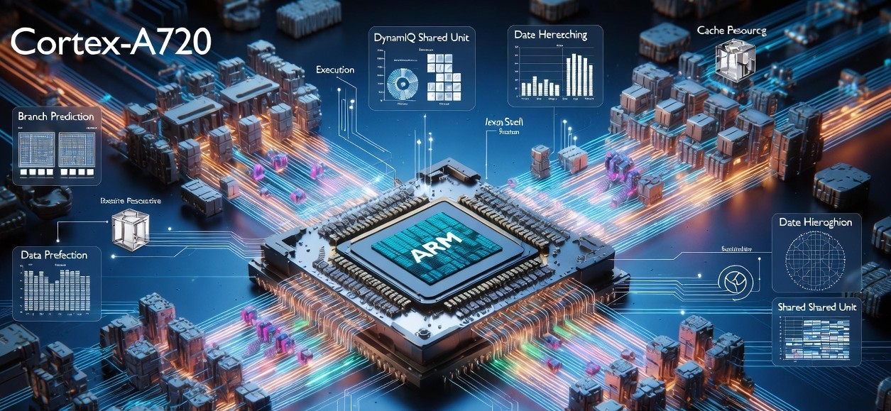
Overview of the ARM Cortex-A720
The ARM Cortex-A720 is a high-performance, efficiency-focused CPU core designed by Arm Holdings, unveiled in May 2023 as part of the company’s Total Compute Solutions 2023 (TCS23) platform. It serves as the successor to the Cortex-A715 and is positioned as a “premium-efficiency” core within Arm’s big.LITTLE heterogeneous computing architecture. This means it strikes a balance between delivering sustained performance for demanding tasks and maintaining low power consumption, making it ideal for mid-tier workloads in multi-core configurations. The Cortex-A720 is built on the Armv9.2 architecture, which is 64-bit only (AArch64), and it emphasizes improvements in power efficiency, security, and machine learning capabilities. It is commonly paired with the high-performance Cortex-X4 core and the ultra-efficient Cortex-A520 core, all managed by the DynamIQ Shared Unit (DSU-120), to form flexible CPU clusters for devices like smartphones, laptops, tablets, and even extended reality (XR) wearables.
Unlike its predecessors, the Cortex-A720 drops support for 32-bit applications, aligning with Arm’s shift toward modern, secure, and efficient computing. This core is engineered to handle sustained high-performance scenarios, such as extended AAA mobile gaming, while operating within tight power envelopes typical of battery-powered devices. Arm claims it provides industry-leading efficiency, with optimizations in branch prediction, data prefetching, and overall microarchitecture that enable better energy use without sacrificing speed. In real-world benchmarks, implementations of the Cortex-A720 have been clocked at around 2.6 GHz to 3.0 GHz, contributing to multi-threaded performance rankings in the mid-to-high tier for mobile processors.
Here is a visual representation of how the Cortex-A720 fits into a typical SoC configuration alongside its sibling cores and the DSU-120:
Key Features and Benefits
The Cortex-A720 incorporates several advanced features that enhance its suitability for modern computing demands:
- Power Efficiency Focus: It achieves a 20% improvement in power efficiency compared to the Cortex-A715 at the same performance level, and a 4.5% performance uplift at the same power consumption (measured on an ISO process). This is accomplished through targeted microarchitecture optimizations, including better branch prediction accuracy and enhanced data prefetching, which reduce unnecessary energy expenditure.
- Security Enhancements: Built on Armv9.2, it includes Memory Tagging Extensions (MTE) for improved memory safety, Reliability, Availability, and Serviceability (RAS) extensions for error handling, and a new QARMA3 algorithm for Pointer Authentication (PAC). These features lower the performance overhead of security measures and strengthen defenses against common exploits like return-oriented programming.
- Machine Learning and Vector Processing: Support for Scalable Vector Extension 2 (SVE2) allows for variable-length vector operations, enabling efficient handling of AI and ML workloads. Arm Neon technology is also included for advanced SIMD (Single Instruction, Multiple Data) processing, accelerating multimedia and computational tasks.
- Cryptography Support: An optional Cryptographic Unit provides hardware acceleration for algorithms like SHA1, SHA256, SHA512, SHA3, SM3, and SM4. This can be controlled via system registers and disabled if needed, making it versatile for secure applications.
- Scalability with DynamIQ: The core integrates seamlessly with the DSU-120, supporting clusters of up to 14 cores. This allows for highly scalable configurations, from single-core wearables to multi-core laptops, with shared L3 cache up to 32MB for better data sharing and reduced latency.
Microarchitecture Details
The Cortex-A720 employs an out-of-order, superscalar pipeline design based on the Armv9.2-A Harvard architecture. This setup allows for efficient execution of instructions by reordering them dynamically to maximize throughput while minimizing stalls.
- Pipeline Structure: The pipeline is out-of-order, enabling the core to execute instructions as soon as their dependencies are resolved, rather than in strict program order. It supports superscalar execution, meaning multiple instructions can be issued, executed, and retired per cycle.
- Cache Hierarchy:
- L1 Instruction and Data Caches: Configurable at 32KB or 64KB each.
- L2 Cache: 128KB, 256KB, or 512KB per core.
- L3 Cache: Optional shared cache ranging from 256KB to 32MB, integrated via the DSU-120 for multi-core efficiency.
- Execution Units: Includes dedicated units for integer, floating-point, and vector operations. The core features a pipelined FDIV/FSQRT unit (borrowed from the Cortex-X4) for faster division and square root operations without increasing area. Faster transfers between NEON/SVE2 and integer units, along with earlier deallocation in Load/Store queues, effectively boost capacity without physical expansions.
- Branch Prediction and Prefetching: Enhanced accuracy in branch prediction reduces misprediction penalties, while improved data prefetching anticipates memory accesses to minimize cache misses.
- Supported Extensions: Up to Armv8.7 extensions, plus Armv9-specific ones like QARMA3, MTE, SVE2, and RAS. Cryptography extensions are optional and include features like FEAT_SHA1 through FEAT_SM4.
- Memory and Addressing: 40-bit physical addressing, with support for Error-Correcting Code (ECC) in caches for reliability. Bus interfaces include AMBA AXI5 or CHI.E, with optional Accelerator Coherency Port (ACP) and Peripheral Port.
- Debug and Monitoring: Includes Performance Monitoring Unit (PMUv3), CoreSightv3 for tracing, and Embedded Trace Extension (ETEv1.0). Activity Monitors Unit (AMU) registers track core activity for power management.
Performance and Efficiency Improvements
Compared to the Cortex-A715, the A720 offers significant gains:
- Efficiency: 20% better power efficiency for the same performance, allowing longer battery life in sustained tasks like gaming or video editing.
- Performance: At identical power levels, it delivers about 4.5% more performance, and in optimized configurations, it can provide increased throughput at the same power as its predecessor.
- Overall System Impact: In a typical 1+5+2 (X4 + A720 + A520) configuration, it contributes to a 27% boost in multi-threaded benchmarks like Geekbench 6 compared to prior generations, even before process node advantages.
These improvements stem from refinements in the core’s inner workings, such as optimized instruction handling and reduced area for equivalent performance (e.g., an area-optimized A720 matches the Cortex-A78’s size but with 10% more performance).
Comparisons to Previous Generations
| Feature | Cortex-A720 | Cortex-A715 | Cortex-A710 |
|---|---|---|---|
| Architecture | Armv9.2-A | Armv9.0-A | Armv8.2-A |
| Power Efficiency Improvement | Baseline | -20% vs. A710 | Baseline for A715 |
| Performance Uplift at Same Power | 4.5% vs. A715 | 20% efficiency vs. A710 | N/A |
| ISA | A64 only | A64 only | A32/A64 |
| Max Clock Speed (Typical) | ~3.0 GHz | ~2.8 GHz | ~2.85 GHz |
| Cluster Size (Max) | 14 cores | 8 cores | 8 cores |
| Extensions | SVE2, MTE, QARMA3 | SVE2, MTE | Limited to Armv8 |
The A720 builds on the A715’s efficiency gains (which were 20% over the A710), compounding to make it substantially more efficient overall.
Use Cases and Applications
The Cortex-A720 is versatile across device categories:
- Smartphones and Tablets: Handles immersive gaming, AI-driven apps, and multitasking with efficient power use.
- Laptops: Provides balanced performance for productivity and content creation in Arm-based Windows or ChromeOS devices.
- Wearables and XR: Supports low-power, sustained operation for augmented reality experiences.
- Cloud and Datacenters: Scales for general-purpose workloads and AI inference, optimizing total cost of ownership.
1) ARM Cortex-A720: Armv9.2-A Microarchitecture Details
The ARM Cortex-A720 employs a modern out-of-order superscalar microarchitecture built on the Armv9.2-A instruction set architecture (AArch64-only, with no 32-bit AArch32 support). This design prioritizes premium efficiency, delivering sustained high performance within tight power constraints typical of mobile, laptop, and embedded SoCs. Arm describes it as the first-generation Armv9.2 premium-efficiency core, focusing on incremental but impactful optimizations rather than radical widening or deepening of the pipeline compared to its predecessor, the Cortex-A715.
The core achieves its headline improvements—approximately 20% better power efficiency at the same performance level and ~4.5% performance uplift at the same power (on an iso-process)—primarily through targeted front-end and memory-system refinements, along with selected back-end enhancements. These include better branch prediction accuracy, improved data prefetching, reduced latencies in critical paths, and efficiency tweaks that avoid unnecessary power burn while preserving (or slightly increasing) throughput.
Pipeline Overview
The Cortex-A720 uses an out-of-order execution pipeline with superscalar dispatch and issue capabilities. While exact stage counts and widths are not publicly disclosed in granular detail (Arm typically reserves full pipeline diagrams for licensees and the Technical Reference Manual), the design follows the evolutionary path of recent Arm “A” series cores:
- It retains a balanced approach similar to the Cortex-A715/A710 lineage, without the aggressive widening seen in “X” series high-performance cores.
- Instruction decode handles Armv9.2-A instructions efficiently, translating them into micro-operations (μops) for out-of-order scheduling.
- The core supports speculative execution with register renaming to hide latencies and maximize instruction-level parallelism.
- Dispatch and issue logic feed execution units, with queues sized to support sustained throughput under mobile workloads.
Key latency reductions contribute to both performance and efficiency:
- Branch misprediction penalty reduced to 11 cycles (from 12 cycles in the Cortex-A715). This single-cycle improvement alone accounts for roughly 1% of observed benchmark gains in many workloads, as mispredictions are expensive (they flush the pipeline and waste energy).
- L2 cache hit latency lowered to 9 cycles (from 10 cycles in the A715), improving data access speed for cache-resident working sets.
These latency optimizations, combined with better prediction and prefetching, allow the core to maintain higher IPC (instructions per cycle) with lower energy expenditure.
Front-End: Instruction Fetch, Decode, and Branch Prediction
The front-end is a major focus area for efficiency gains in the Cortex-A720.
- Branch Prediction — Arm highlights significantly improved branch prediction accuracy as one of the core targeted microarchitecture optimizations. The predictor uses an advanced dynamic mechanism (likely building on prior generations’ two-level adaptive predictors with pattern history tables, global/local history, and tagged structures). It supports processing multiple branches per cycle (with dedicated branch pipelines, often described as handling up to 2 taken branches efficiently). Indirect branch prediction and return stack mechanisms are refined to reduce mispredictions on complex control flow (common in modern code with function pointers, virtual calls, and loops).
- A lower mispredict penalty (11 cycles) further amplifies the benefit of higher accuracy, reducing pipeline flushes and wasted speculation.
- Power optimizations in the prediction logic (e.g., improved 2-taken branch handling) help maintain performance while consuming less energy.
- Instruction Fetch and Decode — The front-end fetches from the L1 instruction cache and decodes into μops. While decode width specifics are not public, the design supports efficient superscalar operation without the 6–8-wide emphasis seen in some prior “big” cores. Prefetching improvements anticipate future instruction streams and data accesses, reducing front-end stalls.
Execution Units and Back-End
The back-end features distinct paths for different operation types, optimized for mobile workloads:
- Integer Execution — Multiple ALUs handle arithmetic, logical, and address-generation operations. The design includes enhancements for faster integer multiply-accumulate (MAC) patterns.
- Load/Store Unit — Dedicated load/store pipelines with improved queue management. Earlier deallocation from load/store queues effectively increases effective queue capacity without physical area growth, allowing more outstanding memory operations.
- Floating-Point and Vector Units — Handles scalar FP, NEON (Advanced SIMD), and SVE2 (Scalable Vector Extension 2) instructions. A key addition is a pipelined FDIV/FSQRT unit (borrowed from the Cortex-X4 lineage), accelerating floating-point divide and square-root operations without significant area penalty.
- Faster data transfers between NEON/SVE2 vector registers and integer/general-purpose registers reduce latency when mixing scalar and vector code (common in ML inference, graphics, and multimedia).
- Overall, the back-end focuses on sustained throughput rather than peak burst width, aligning with the core’s efficiency mandate.
Cache Hierarchy and Memory System
The memory subsystem is configurable for area/power/performance trade-offs:
- L1 Instruction Cache — 32 KB or 64 KB (with parity/ECC options for reliability).
- L1 Data Cache — 32 KB or 64 KB (Harvard architecture, separate I$ and D$).
- L2 Cache — Private per-core cache of 128 KB, 256 KB, or 512 KB. Bandwidth is doubled compared to the Cortex-A715 in some configurations, and hit latency is reduced to 9 cycles.
- L3 Cache — Shared via the DSU-120 (DynamIQ Shared Unit), configurable up to 32 MB (increased from prior DSU generations’ typical 16 MB max), supporting clusters of up to 14 cores.
- Prefetching — Enhanced hardware data prefetcher anticipates memory access patterns more accurately, reducing effective miss rates and stalls.
- Physical Addressing — 40-bit, with support for large pages and ECC in caches.
- Interconnect — Interfaces via AMBA CHI or AXI5 coherent buses, with optional Accelerator Coherency Port (ACP).
These cache improvements, combined with better prefetching, significantly boost efficiency for memory-bound workloads like gaming, browsing, and AI inference.
Additional Microarchitectural Features
- Out-of-Order Reordering Capacity — Sufficient reorder buffer (ROB) and issue queue sizes to hide long latencies (e.g., cache misses, divides).
- Security Features — Hardware support for Memory Tagging Extensions (MTE), Pointer Authentication (QARMA3 algorithm) with reduced overhead, RAS extensions, and optional cryptography acceleration (SHA, AES, SM3/SM4).
- Debug and Monitoring — Performance Monitors (PMU), CoreSight trace, Activity Monitors (AMU), and Statistical Profiling Extension (SPE) support.
- Area-Optimized Variant — An alternative configuration matches the Cortex-A78’s silicon footprint while delivering ~10% higher performance at iso-power, useful for cost-sensitive designs.
In summary, the Cortex-A720’s microarchitecture refines rather than revolutionizes the A715 foundation. By focusing on front-end accuracy (branch prediction, prefetching), latency reductions (mispredict recovery, L2 hits), and selective back-end accelerations (pipelined FP ops, faster vector-integer bypass), it achieves meaningful efficiency gains without increasing complexity or area in most configurations. This makes it particularly well-suited for sustained, power-constrained workloads in modern heterogeneous SoCs.
1.1) Microarchitecture: Out-of-order superscalar pipeline
The ARM Cortex-A720 features an out-of-order superscalar pipeline optimized for premium efficiency, building directly on the foundation established in prior premium-efficiency cores like the Cortex-A715. Unlike Arm’s high-performance “X” series cores (e.g., Cortex-X4), which often receive aggressive increases in pipeline width, depth, or reordering capacity, the Cortex-A720 prioritizes targeted tuning to eliminate power-wasting bottlenecks, reduce critical latencies, and improve prediction accuracy. This results in its headline 20% power efficiency gain at the same performance level (or ~4.5% performance uplift at the same power) compared to the Cortex-A715, achieved largely through front-end and memory-system refinements rather than fundamental widening or lengthening of the pipeline.
Arm has explicitly stated that there is no change in the architectural width and depth of the Cortex-A720 compared to the Cortex-A715. The focus instead lies on microarchitectural optimizations that remove inefficiencies, lower energy per useful operation, and deliver measurable real-world benefits in sustained workloads typical of mobile and laptop devices.
High-Level Pipeline Structure
The Cortex-A720 implements a classic modern Arm out-of-order pipeline with the following logical stages (typical of recent A-series premium-efficiency cores, though exact internal stage counts are not publicly detailed beyond high-level descriptions):
- Front-End Stages:
- Branch Prediction + Instruction Fetch: Instructions are predicted and fetched from the L1 instruction cache (configurable 32 KB or 64 KB). The front-end supports efficient handling of multiple instructions per cycle, with enhanced mechanisms for processing two taken branches in a power-efficient manner.
- Instruction Align and Decode: Fetched instructions (Armv9.2-A A64 only) are aligned and decoded into macro-operations (MOPs). These MOPs may be further broken down into micro-operations (μops) for more granular scheduling and execution. Decode supports superscalar operation, though Arm does not publicly specify an exact decode width increase over the A715 (prior generations like A715 featured improvements to 5-way decode in some contexts, but A720 maintains similar effective capability without major expansion).
- Rename and Dispatch: Register renaming eliminates false dependencies (WAR/WAW hazards), and renamed μops are dispatched to issue queues and reservation stations. Dispatch feeds the out-of-order engine.
- Back-End Stages:
- Issue and Execute: μops are issued out-of-order from queues to appropriate execution units when operands are ready. Execution occurs across parallel pipelines for different operation types.
- Writeback and Retire: Results are written back to the register file (or forwarded), and instructions are retired in program order once all prior instructions have completed and no exceptions remain.
The pipeline supports speculative execution with recovery on mispredictions or exceptions. The overall design emphasizes low-latency recovery paths and reduced energy on speculation failures, which is critical for efficiency in battery-constrained environments.
Key Pipeline Metrics and Improvements
While Arm does not publish a full stage-by-stage diagram or exact cycle counts for every internal path (detailed internals are typically in the licensee-only Technical Reference Manual), several concrete metrics highlight the pipeline refinements in the Cortex-A720:
- Branch Misprediction Penalty — Reduced to 11 cycles (from 12 cycles in the Cortex-A715). This one-cycle shave in recovery time provides meaningful gains in real applications, as branch mispredictions flush the pipeline and waste energy on discarded speculative work. Even small reductions here compound across billions of branches in typical code, contributing to both performance and efficiency.
- L2 Cache Hit Latency — Lowered to 9 cycles (from 10 cycles in the A715). Faster access to the private L2 cache (configurable 128 KB, 256 KB, or 512 KB) reduces stalls when data misses the L1 caches, improving effective IPC (instructions per cycle) without increasing power draw.
- Two-Taken Branch Handling — Further optimized for power efficiency. The predictor now handles scenarios with two consecutive taken branches more accurately and with lower energy cost, without sacrificing throughput. This builds on prior generational improvements in branch prediction structures (e.g., better pattern recognition, tagged predictors, and return stack mechanisms).
- Pipeline Depth and Width — No increase in overall depth or dispatch/issue width compared to the A715. The core retains a balanced superscalar design suited to sustained rather than peak-burst workloads. This conservative approach avoids the power and area penalties of deeper/wider pipelines while still delivering incremental gains through tuning.
Execution Resources and Back-End Details
The back-end remains focused on mobile-relevant operation mixes:
- Integer Execution — Multiple ALUs for arithmetic, logical, and address generation, with efficient handling of common patterns like multiply-accumulate.
- Load/Store Unit — Dedicated pipelines with improved queue management. Earlier deallocation from load/store queues increases effective capacity for outstanding memory operations without physical expansion.
- Floating-Point and Vector — Pipelined units supporting scalar FP, NEON (128-bit SIMD), and SVE2 (scalable vectors). A notable addition is a fully pipelined FDIV/FSQRT unit (inherited/refined from Cortex-X4 influences), which accelerates divide and square-root operations without meaningful area increase. Faster bypass paths between vector/NEON and integer units reduce latency when code mixes scalar and vector instructions (common in ML, graphics, and media processing).
The out-of-order window (reorder buffer and related structures) provides sufficient capacity to hide long latencies (e.g., cache misses or multi-cycle operations), though it is not expanded aggressively like in “X” cores.
Why These Changes Matter
The Cortex-A720’s pipeline refinements exemplify Arm’s efficiency-first philosophy for mid-tier cores:
- Lower mispredict and cache-hit latencies reduce wasted cycles and energy.
- Better branch prediction and prefetching keep the front-end fed efficiently.
- Selective accelerations (e.g., pipelined FP divide) target real bottlenecks without broad complexity increases.
In practice, these yield sustained performance closer to theoretical peaks in power-constrained scenarios, such as prolonged gaming sessions, multitasking, or AI inference on smartphones and laptops. The lack of major width/depth changes keeps implementation area and power overhead manageable, allowing SoC designers to scale clusters (up to 14 cores via DSU-120) while meeting thermal and battery targets.
For the most authoritative and granular details—including exact internal stage breakdowns, reorder buffer sizes, issue queue depths, or full execution port mappings—refer to Arm’s Cortex-A720 Technical Reference Manual (TRM), available exclusively to licensed partners through developer.arm.com. Public disclosures remain intentionally high-level to protect implementation IP while highlighting the efficiency-focused evolution from the Cortex-A715.
1.2) Microarchitecture: Cache Hierarchy and Memory System
The ARM Cortex-A720 features a sophisticated, configurable cache hierarchy and memory system designed to deliver high sustained performance with excellent power efficiency in mobile, laptop, and embedded SoCs. The design follows a classic multi-level cache approach typical of modern Arm premium-efficiency cores: separate L1 instruction and data caches (Harvard architecture), a private unified L2 cache per core, and an optional shared L3 cache provided through the DynamIQ Shared Unit (DSU-120). This hierarchy minimizes average memory access latency, reduces DRAM traffic, and supports efficient data sharing in multi-core clusters while incorporating reliability features like ECC and advanced prefetching.
Arm emphasizes configurability, allowing SoC designers to trade off silicon area, power, and performance based on target device constraints (e.g., smartphones vs. laptops). The memory system integrates tightly with the out-of-order execution engine, enabling the core to hide latencies effectively through outstanding misses, prefetching, and optimized bypass paths.
L1 Cache (Level 1)
The L1 cache uses a Harvard architecture with physically separate instruction cache (I-cache) and data cache (D-cache). This separation optimizes for different access patterns: instruction fetches are typically sequential and predictable, while data accesses are more random and require low-latency support for load/store operations.
- Sizes — Configurable as 32 KB or 64 KB for each (I-cache and D-cache independently selectable in many implementations).
- Associativity — Typically 4-way set-associative (common for Arm A-series L1 caches in this generation).
- Line Size — 64 bytes (standard Arm cache line size, balancing bandwidth and tag overhead).
- Error Protection —
- Parity on L1 I-cache (single-error detection).
- ECC (Error-Correcting Code) options on L1 D-cache, supporting Single Error Correction, Double Error Detection (SECDED) for higher reliability in safety-critical or server-like applications.
- Access Latency — Very low (typically 3–4 cycles, though exact internal cycle count is implementation-specific and not publicly detailed beyond high-level descriptions).
- Key Optimizations — The L1 system includes a doubled Translation Lookaside Buffer (TLB) capacity in some configurations (inherited/refined from prior generations), reducing page table walk penalties on TLB misses. Bank conflict improvements further enhance effective bandwidth for concurrent loads/stores.
The L1 hierarchy keeps most hot code and data close to the execution units, minimizing pipeline stalls in bursty mobile workloads like app launches, gaming, or browsing.
L2 Cache (Level 2)
Each Cortex-A720 core has a dedicated, private unified L2 cache that serves both instructions and data (von Neumann style at this level). This private L2 acts as the primary victim cache for L1 misses and provides significantly higher capacity than L1 while maintaining reasonable latency.
- Sizes — Configurable as 128 KB, 256 KB, or 512 KB per core (most common implementations use 256 KB or 512 KB for balanced performance).
- Associativity — 8-way set-associative (provides good hit rates without excessive tag/power overhead).
- Line Size — 64 bytes (consistent with L1).
- Error Protection — Optional ECC with SECDED on the L2 cache itself, plus Single Error Detection (SED) on the L2 TLB.
- Hit Latency — Reduced to 9 cycles (down from 10 cycles in the Cortex-A715). This one-cycle improvement is significant: it directly reduces the penalty for L1 misses, boosting effective IPC (instructions per cycle) and lowering energy spent waiting for data.
- Bandwidth Improvements — Up to 2× bandwidth in certain operations (e.g., memset-like patterns), achieved through wider internal paths and optimized arbitration.
- Prefetching — Enhanced with a new L2 spatial-prefetch engine (borrowed/refined from high-performance Cortex-X lineage). This predicts and prefetches adjacent cache lines based on observed access patterns, improving hit rates for streaming or strided workloads (e.g., multimedia, AI inference, gaming textures).
- Other Features — Supports earlier deallocation from load/store queues (increasing effective outstanding miss capacity) and faster store data availability.
The L2 refinements contribute substantially to the core’s 20% power efficiency gain over the A715 by reducing DRAM accesses and shortening stall cycles without increasing area disproportionately.
L3 Cache (Level 3) and System-Level Integration
The L3 cache is shared across all cores in a DynamIQ cluster, managed by the DSU-120 (DynamIQ Shared Unit, updated for Armv9.2-era cores).
- Sizes — Optional, configurable from 256 KB up to 32 MB (a doubling from prior DSU generations’ typical 16 MB max). Common real-world implementations use 4–16 MB in flagship mobile SoCs, with larger sizes (e.g., 24 MB or 32 MB) possible in laptops or premium tablets.
- Organization — Sliced (typically 8 slices for larger configurations), with power gating and retention modes to save energy when idle.
- Coherency — Fully coherent via Arm’s CHI (Coherent Hub Interface) or AXI5 protocols. The DSU-120 includes snoop control units and supports intra-cluster coherence for fast data sharing between cores (e.g., producer-consumer patterns in multi-threaded apps).
- Additional Features —
- Memory System Resource Partitioning and Monitoring (MPAM) for quality-of-service in heterogeneous environments.
- Opportunistic power modes (e.g., L3 half-on, low-power data retention, slice-level toggling) to minimize leakage in light workloads.
- Optional Accelerator Coherency Port (ACP) for direct coherent access by peripherals or accelerators.
The larger maximum L3 size improves multi-core scaling (up to 14 cores per cluster, up from 12 in prior DSUs) and reduces inter-core communication latency, benefiting sustained multi-threaded performance in gaming, video editing, or AI tasks.
Overall Memory System Characteristics
- Physical Addressing — Up to 40 bits (sufficient for large DRAM capacities in modern devices).
- Bus Interfaces — AMBA CHI.E (preferred for high-performance coherent systems) or AXI5, enabling integration with Arm’s CMN (Coherent Mesh Network) interconnects for system-level scaling.
- Prefetching and Latency Hiding — Hardware prefetchers at L1 and L2 levels (including the new L2 spatial prefetcher) anticipate future accesses, reducing effective miss penalties. The out-of-order engine tracks multiple outstanding misses to DRAM.
- Reliability — Comprehensive ECC/Parity across levels, plus RAS (Reliability, Availability, Serviceability) extensions for advanced error handling and reporting.
- Power Management — Tight integration with DSU-120 power modes allows dynamic cache sizing/power gating, crucial for battery life in sustained workloads.
Comparison to Predecessor (Cortex-A715)
| Feature | Cortex-A720 | Cortex-A715 | Improvement/Change |
|---|---|---|---|
| L1 I/D /D /D Sizes | 32 KB or 64 KB each | 32 KB or 64 KB each | Same (configurable) |
| L2 Size | 128–512 KB | 128–512 KB | Same, but with optimizations |
| L2 Hit Latency | 9 cycles | 10 cycles | -1 cycle (key efficiency gain) |
| L2 Bandwidth | Up to 2× in key ops | Baseline | Improved for common patterns |
| L3 (via DSU) | Up to 32 MB | Up to 16 MB (typical) | Doubled max capacity |
| Cluster Size | Up to 14 cores (DSU-120) | Up to 12 cores | +2 cores for better scaling |
| Prefetch Enhancements | New L2 spatial prefetcher | Prior prefetchers | Better anticipation, fewer misses |
In summary, the Cortex-A720’s cache hierarchy and memory system represent evolutionary but impactful refinements: lower L2 latency, enhanced prefetching, doubled L3 capacity potential, and robust error protection. These changes compound to deliver the core’s claimed efficiency and sustained performance advantages, making it well-suited for power-constrained, long-running tasks in next-generation devices. For precise implementation-specific details (e.g., exact associativity, replacement policies, or internal queue depths), consult Arm’s Cortex-A720 Technical Reference Manual (TRM), available to licensees via developer.arm.com.
1.3) Microarchitecture: Memory Tagging Extensions (MTE)
Memory Tagging Extensions (MTE) is a hardware-based security feature in the Arm architecture designed to detect and mitigate common memory safety vulnerabilities in software, particularly in languages like C and C++ that allow direct memory management. MTE significantly enhances memory safety by catching errors such as buffer overflows, use-after-free, use-after-return, double-free, and certain forms of heap corruption at runtime with relatively low performance overhead compared to software-based alternatives like AddressSanitizer (ASan).
Introduced as part of the Armv8.5-A architecture extension in 2019, MTE became a core component of the Armv9 family (including Armv9.0-A and later versions such as Armv9.2-A used in the Cortex-A720). In the Cortex-A720, MTE is always implemented (mandatory, not optional), making the core fully compliant with protocols like CHI.E that support tagged memory coherency. This ensures consistent behavior across heterogeneous clusters (e.g., Cortex-X4 + A720 + A520 configurations).
Core Concept: The “Lock and Key” Mechanism
MTE operates on a probabilistic “lock and key” model for memory accesses:
- Memory Tagging (Lock): Physical memory is divided into small granules of 16 bytes each. Every granule is assigned a 4-bit tag (0–15, providing 16 possible tags). This tag is stored in dedicated tag memory (separate from the main DRAM array, typically in a small on-chip structure or alongside the L2/L3 cache in implementations).
- Pointer Tagging (Key): When a pointer is created (e.g., during malloc() or similar allocation), the same 4-bit tag is embedded into the pointer itself. Arm leverages the Top Byte Ignore (TBI) feature in AArch64, where the top byte (bits 56–63) of a 64-bit virtual address is ignored by address translation. MTE uses the lower nibble (4 bits) of this top byte to store the tag, leaving the upper nibble for other uses if needed.
- Runtime Checking: On every load or store instruction, the CPU compares the tag in the pointer (key) against the tag stored for the accessed memory granule (lock). If they match, the access proceeds normally. If they mismatch, the hardware can:
- Raise a synchronous fault (immediate exception, precise reporting of the faulting instruction).
- Log the error asynchronously (deferred reporting).
- Or ignore it (in some modes).
This check happens in hardware with minimal latency, making MTE far more efficient than software instrumentation.
Granularity and Probabilistic Nature
- Tags apply to 16-byte aligned granules, meaning MTE detects overflows or underflows that cross granule boundaries with high probability.
- With only 16 possible tags, collisions are possible (two unrelated allocations could share the same tag). This makes MTE probabilistic rather than deterministic—unlike full shadow-memory sanitizers—but the low tag space is a deliberate trade-off for negligible overhead.
- Allocators (e.g., in the Linux kernel, Android’s libc, or custom heaps) must assign fresh, random tags on allocation and invalidate/re-tag on deallocation to maximize detection probability.
MTE Operating Modes
MTE supports multiple modes, configurable via system registers (e.g., PSTATE.TCO for tag checking override, or TCR_ELx for global control):
- Synchronous Mode (SYNC) — Tag mismatches cause an immediate synchronous fault (precise exception). This mode provides excellent debuggability (exact instruction and address reported) but has higher overhead (~5–20% in typical workloads, depending on access density). Ideal for development, testing, and fuzzing.
- Asynchronous Mode (ASYNC) — Mismatches are deferred and reported only after a context switch or explicit check instruction. This mode has very low overhead (often <5%) and is suitable for production hardening, though it loses precise fault location information.
- Asymmetric Mode (ASYMM or Asymmetric MTE) — Introduced in later Armv9 generations (refined in cores like Cortex-A715/A720 lineage). It offers a hybrid: some accesses use strict synchronous checking, while others use lighter asynchronous or selective checking. This provides tunable trade-offs between precision, speed, and coverage, enabling broader ecosystem adoption.
In the Cortex-A720 (Armv9.2-A), all modes are supported, with hardware optimizations reducing the cost of tag checks and tag storage/access.
Integration with Cortex-A720
- The Cortex-A720 always implements MTE (as confirmed in its Technical Reference Manual), ensuring full support in Armv9.2-based SoCs (e.g., Google Tensor G4 in Pixel 9, certain MediaTek Dimensity, and others).
- Tag storage and checking are integrated into the memory system, with coherency maintained across L1/L2/L3 caches and system interconnects (via CHI.E protocol).
- Performance studies (e.g., on Pixel 9 with A720 cores) show MTE overhead remains low in real workloads, especially in ASYNC or ASYMM modes, making it viable for production use.
- Android support: From Android 14 onward, MTE is exposed as a developer option on compatible devices (Settings > Developer Options > Memory Tagging Extension), allowing per-app or system-wide enabling for testing.
Benefits and Limitations
- Benefits:
- Detects a wide range of memory safety bugs (spatial and temporal) that traditional mitigations (ASLR, stack canaries, etc.) miss.
- Hardware-enforced → minimal runtime cost compared to software sanitizers.
- Probabilistic but effective: random tag assignment makes reliable exploitation much harder.
- Supports both debugging (SYNC) and production hardening (ASYNC/ASYMM).
- Complements other Armv9 features like Pointer Authentication (PAC) and Branch Target Identification (BTI).
- Limitations:
- Probabilistic (16 tags → ~1/16 chance of missing a specific corruption if tags collide).
- Requires allocator modifications (kernel, libc, or app heaps) to set and propagate tags correctly.
- Not foolproof against all attacks; research has shown theoretical bypasses (e.g., tag guessing in specific scenarios), though Arm views tags as non-secret metadata.
- Adoption varies: While Cortex-A720 supports it fully, some SoCs (e.g., certain Snapdragon implementations) disable or omit MTE in silicon.
In summary, MTE in the Cortex-A720 represents Arm’s most advanced hardware approach to memory safety in premium-efficiency cores. It shifts detection of critical vulnerabilities from software overhead to near-zero-cost hardware checks, enabling safer native code execution in mobile, laptop, and embedded environments.
1.4) Microarchitecture: Pointer Authentication (PAC) with the QARMA3 algorithm
Pointer Authentication (PAC) with the QARMA3 algorithm is an advanced hardware-enforced security mechanism in the Arm architecture, specifically enhanced in Armv9.2-A (the architecture implemented by the Cortex-A720). Pointer Authentication protects against memory corruption exploits—such as return-oriented programming (ROP), jump-oriented programming (JOP), and certain data pointer attacks—by cryptographically signing (authenticating) pointers before they are stored or used. This makes it extremely difficult for attackers to forge valid pointers, even if they can corrupt memory.
Introduced in Armv8.3-A (using the original QARMA algorithm), PAC has evolved through refinements like QARMA5 and now QARMA3 in Armv9.2. The Cortex-A720 implements FEAT_PACQARMA3 (Pointer Authentication using the QARMA3 algorithm), as confirmed in its Technical Reference Manual. This feature is mandatory in Armv9.2-compliant cores like the A720, ensuring full support for enhanced pointer integrity with significantly reduced performance overhead compared to earlier implementations.
Core Mechanism: How Pointer Authentication Works
PAC operates on a “sign-then-verify” model for pointers (both code/instruction pointers and data pointers):
- Signing (PAC generation): When a pointer is created or stored (e.g., during function call setup for a return address or when storing a function pointer), the CPU computes a short Pointer Authentication Code (PAC). This PAC is a cryptographic Message Authentication Code (MAC) derived from:
- The pointer value itself (the virtual address bits that matter).
- A 64-bit context value (typically the stack pointer SP or a similar value to bind the pointer to its usage context, preventing reuse attacks).
- One of several secret 128-bit keys managed by privileged software.
- Verification (AUT): Before the pointer is dereferenced or used (e.g., on function return or indirect branch), the CPU recomputes the expected PAC using the same inputs (pointer bits + context + key) and compares it to the embedded PAC. If they match, the pointer is considered authentic and the access proceeds. If they mismatch, the hardware raises a fault (typically an Instruction Abort or Data Abort), preventing execution of corrupted control flow.
- Key Separation: Arm defines five independent 128-bit keys:
- APIAKey and APIBKey — for instruction (code) pointers (A/B variants for diversity).
- APDAKey and APDBKey — for data pointers.
- A general-purpose key — used by the PACGA instruction for computing authentication codes over arbitrary data (e.g., heap metadata protection).
- Supporting Instructions (AArch64):
- PAC family* (e.g., PACIA, PACIB, PACDA, PACDB) — generate PAC and insert it.
- AUT family* (e.g., AUTIA, AUTIB, AUTDA, AUTDB) — authenticate and strip PAC if valid.
- Combined forms — e.g., RETA (authenticate then return), BLRAA (branch with link and authenticate).
- XPAC* — strip PAC without checking (for debugging or trusted code).
- PACGA — general-purpose MAC computation (32-bit output) over two 64-bit inputs.
This mechanism hardens control-flow integrity (CFI) and data pointer integrity at the hardware level, complementing software mitigations like stack canaries, ASLR, and DEP/NX.
The QARMA3 Algorithm in Armv9.2
The original PAC (Armv8.3) used the QARMA family of lightweight tweakable block ciphers, designed by Qualcomm specifically for short-tag MAC generation with low latency in hardware.
QARMA3 (introduced in Armv9.2) is a further optimized variant of this cipher family, tailored to reduce the computational and power overhead of PAC operations—especially important for efficiency-focused cores like the Cortex-A720 and even more so for in-order cores like the Cortex-A520.
Key improvements with QARMA3:
- Drastically reduced overhead: Arm claims QARMA3 brings the performance cost of enabling PAC to less than 1% in typical workloads, even on smaller/efficiency cores. Earlier QARMA implementations had noticeably higher overhead (often 5–15% in some cases), limiting widespread adoption in production systems.
- Cryptographic strength for truncated tags: PAC tags are short (typically 11–31 bits depending on virtual address size and whether TBI is used), so the algorithm must remain secure even after heavy truncation. QARMA3 retains the reflection-based, conservative S-box design of prior QARMA variants while optimizing for lower cycle count and energy in unrolled hardware implementations.
- Better suitability for in-order and efficiency cores: The lower latency and reduced complexity make PAC viable without compromising the power-efficiency goals of cores like A720/A520.
In the Cortex-A720:
- FEAT_PACQARMA3 is explicitly supported (alongside FEAT_PACIMP for implementation-defined algorithms and FEAT_CONSTPACFIELD for PAC enhancements).
- The core can also support related features like FEAT_PAuth2 (enhanced PAC) in some configurations.
- This enables near-zero-cost pointer signing/verification in real-world mobile and laptop workloads, making it practical to enable system-wide in OSes like Android or Linux.
Benefits and Real-World Impact
- Mitigates major exploit classes — ROP/JOP attacks become much harder because forged return addresses or function pointers fail authentication.
- Complements Armv9 security suite — Works alongside Memory Tagging Extensions (MTE) for memory safety and Branch Target Identification (BTI) for indirect branch protection.
- Minimal performance hit — With QARMA3, the overhead drops below 1%, encouraging broader enablement in consumer devices (e.g., smartphones, laptops) without noticeable battery or speed penalties.
- Probabilistic but effective hardening — Like many MAC-based schemes, security relies on secret keys and cryptographic strength; short tags mean theoretical collision risks exist, but the design makes practical attacks extremely difficult.
Limitations and Considerations
- Requires OS/kernel support to initialize keys, instrument code (e.g., via compiler flags like -mbranch-protection=pac-ret), and handle faults.
- Not immune to all side-channel or speculative-execution attacks (research has explored theoretical bypasses like PACMAN-style speculation, though mitigations exist).
- Probabilistic nature (short tags) means it’s not 100% deterministic like full pointer encryption, but the combination of secret keys and context binding provides strong practical protection.
In the Cortex-A720, QARMA3-powered Pointer Authentication represents Arm’s continued push toward hardware-rooted security that is both robust and efficient enough for everyday devices. This allows next-generation SoCs to deliver stronger defenses against memory corruption vulnerabilities while preserving the core’s focus on sustained performance and battery life.
1.5) Microarchitecture: Debug and monitoring
The ARM Cortex-A720 includes a comprehensive suite of debug and monitoring features aligned with the Armv9.2-A architecture and the broader Arm CoreSight framework. These capabilities enable developers, silicon bring-up teams, OS/kernel engineers, and performance analysts to observe, control, profile, and trace core behavior at various privilege levels (EL3, EL2, EL1, EL0) with minimal intrusion. The design supports both invasive debug (halting the core, stepping, breakpoints) and non-invasive monitoring (profiling, event counting, instruction/data tracing) while preserving the core’s efficiency focus.
All debug features comply with Arm’s CoreSight architecture, allowing seamless integration into multi-core SoCs via the Debug Access Port (DAP) (typically SWD or JTAG) and interconnects like AMBA CHI/AXI. The Cortex-A720 implements Armv9.2-A debug logic as baseline, with several optional but commonly included extensions.
Core Debug Features (Invasive Debug)
These provide traditional debugger control over the core:
- Armv9.2-A Debug Logic — Full support for the Armv9 debug architecture, including:
- Halt, single-step, and resume control.
- Software breakpoints (via BKPT instruction) and hardware breakpoints/watchpoints.
- Access to core registers (general-purpose, floating-point/SVE2, system registers) at all exception levels.
- Debug state entry/exit handling, including secure vs. non-secure world separation.
- Debug authentication signals (e.g., DBGEN, SPIDEN, NIDEN, SPNIDEN) to gate debug access based on security policy.
- Precise exception reporting and fault injection for testing.
- Breakpoints and Watchpoints — Multiple hardware units (typically 6–8 breakpoints and 4–8 watchpoints, configurable per implementation) for address, context, or data-value matching. Supports EL2/EL3 virtualization-aware breakpoints.
Performance Monitoring Unit (PMU)
The Performance Monitoring Unit (PMU) is a key non-invasive monitoring component, compliant with the Armv8 PMU architecture (extended for Armv9).
- Purpose — Counts architectural and microarchitectural events (e.g., instructions retired, cycles, cache misses, branch mispredictions, TLB walks, pipeline stalls, SVE2 vector operations, memory system events).
- Implementation — Multiple 64-bit event counters (typically 32+ programmable counters, plus fixed-function counters for cycles and instructions).
- Features:
- Event filtering by exception level (EL0/EL1/EL2/EL3) and secure/non-secure state.
- Overflow interrupts for sampling/profiling.
- Chainable counters for 128-bit counts on high-frequency events.
- Support for MPAM (Memory System Resource Partitioning and Monitoring) integration, allowing QoS-aware performance monitoring in partitioned systems.
- Use Cases — Real-time profiling, bottleneck identification (e.g., memory-bound vs. compute-bound workloads), power/performance tuning in mobile/laptop SoCs.
Activity Monitors Unit (AMU)
The Activity Monitors Extension (introduced in Armv8.4-A, fully supported in Cortex-A720) provides fixed, low-overhead counters for high-level activity tracking.
- Implementation — Seven 64-bit counters organized in two groups:
- Group 0: Four counters (0–3) tracking fixed events (e.g., constant frequency cycles, core active cycles).
- Group 1: Additional counters for implementation-specific or extended activity (e.g., sleep states, power modes).
- Purpose — Lightweight monitoring of core utilization and power-related activity without the full configurability (and overhead) of the PMU.
- Use Cases — OS-level scheduling decisions, thermal/power management, estimating energy consumption per task.
Trace Features (Non-Invasive Instruction and Data Tracing)
The Cortex-A720 integrates modern CoreSight trace components for capturing program flow and data accesses in real time:
- Embedded Trace Extension (ETE) — The primary instruction trace unit, replacing older ETM/PTM in Armv9 cores.
- Captures branch traces, exceptions, and instruction execution flow.
- Supports Armv9 instruction set (AArch64 only) with efficient compression.
- Configurable trace modes (e.g., full trace, sample-based, address-range filtering).
- Low-overhead for always-on or selective tracing.
- TRace Buffer Extension (TRBE) — On-chip trace buffer for storing ETE trace data locally.
- Allows capture without immediate off-chip streaming (useful when trace port bandwidth is limited).
- Supports wrap-around, fill-to-trigger, and halt-on-full modes.
- Statistical Profiling Extension (SPE) — Optional — Probabilistic sampling of instructions and memory accesses.
- Captures detailed samples (PC, virtual/physical address, latency, events) at configurable intervals.
- Enables low-overhead hotspot detection, cache miss profiling, and memory access pattern analysis.
- Data streamed via CoreSight ATB (AMBA Trace Bus) or stored in TRBE.
- Embedded Logic Analyzer (ELA-600) — Optional (licensed separately) — Advanced on-chip logic analyzer for custom signal probing and triggering.
- Useful for silicon validation and low-level hardware debugging.
Integration with CoreSight Infrastructure
All trace and debug components connect via the CoreSight framework:
- Debug Access Port (DAP) — Entry point for external debuggers (SWD/JTAG).
- Trace Bus (ATB) — High-bandwidth transport for trace data to off-chip ports (e.g., TPIU, HSSTP) or on-chip sinks (ETB/ETF/ETR).
- Cross Trigger Interface (CTI/CTM) — Synchronize debug/trace events across cores or with peripherals.
- Trace Port Interface Unit (TPIU) — Off-chip export (parallel or serial).
This allows full-system debug/trace in heterogeneous clusters (e.g., Cortex-X4 + A720 + A520) managed by DSU-120.
Comparison of Key Monitoring Components
| Component | Type | Primary Purpose | Overhead | Configurability | Typical Use Case |
|---|---|---|---|---|---|
| PMU | Event counters | Detailed performance event counting | Low–medium | High | Profiling, bottleneck analysis |
| AMU | Fixed counters | Core activity & power-state monitoring | Very low | Low | OS power management, utilization |
| ETE + TRBE | Instruction trace | Full/conditional program flow capture | Medium (trace) | High | Code coverage, bug reproduction |
| SPE (optional) | Statistical sample | Probabilistic instruction/memory sampling | Very low | Medium | Hotspot detection, memory profiling |
| ELA-600 | Logic analyzer | Custom signal/event triggering | Variable | Very high | Silicon validation, hardware debug |
In summary, the Cortex-A720’s debug and monitoring suite provides a powerful, standards-compliant toolkit for development, optimization, and validation. The combination of PMU, AMU, ETE/TRBE, and optional SPE delivers both deep visibility (via trace) and lightweight always-on monitoring (via counters), all while supporting Arm’s shift toward secure, efficient Armv9 systems.
1.6) Microarchitecture: Reliability, Availability, and Serviceability (RAS) Extensions
The ARM Cortex-A720 implements the Reliability, Availability, and Serviceability (RAS) Extensions as a mandatory architectural feature of its Armv9.2-A base. RAS is a framework introduced in Armv8.2-A (and mandatory from Armv8.2 onward for many profiles) to detect, report, contain, and recover from hardware errors in a structured, predictable way. This is especially valuable in modern heterogeneous SoCs where soft errors (e.g., from cosmic rays, voltage droops, or aging silicon) become more probable at advanced process nodes, and where sustained reliability matters for consumer devices, automotive, edge computing, and even some datacenter workloads.
Arm explicitly lists RAS extensions among the supported features of the Cortex-A720 in its official product documentation, product briefs, and the Cortex-A720 Core Technical Reference Manual (TRM, document 102530). The core supports RAS Extension version 1.1, along with full containment capability for all extensions up to Armv9.0-A (and compatible with Armv9.2 updates). This means the Cortex-A720 provides hardware mechanisms to handle error detection and signaling in line with the latest Arm RAS System Architecture.
What Are RAS Extensions?
RAS defines a standardized architecture for error handling across Arm systems, moving away from ad-hoc vendor-specific mechanisms toward a unified model. Key goals include:
- Reliability — Reducing the probability and impact of undetected or unrecoverable errors.
- Availability — Enabling systems to continue operating (possibly in degraded mode) after recoverable errors.
- Serviceability — Providing detailed error information for diagnostics, logging, predictive maintenance, and failure analysis.
The RAS architecture organizes errors into nodes (components like caches, TLBs, interconnects, memory controllers) and uses Error Records to log faults. It supports multiple containment levels:
- Uncontained errors — Catastrophic; typically require a full system reset.
- Contained errors — Recoverable by software/firmware without full reset (e.g., via poison propagation or retry).
- Deferred errors — Detected but not immediately fatal; handled later.
RAS Support in the Cortex-A720
The Cortex-A720 integrates RAS at the core level and coordinates with the surrounding DynamIQ Shared Unit (DSU-120) and system-level components. Specific aspects include:
- Error Detection Mechanisms —
- ECC (Error-Correcting Code) / Parity protection on internal structures (L1 instruction/data caches, L2 cache, and optionally other arrays). The Cortex-A720 supports configurable ECC/parity on caches, allowing correction of single-bit errors and detection of multi-bit errors.
- Hardware detection of faults in execution units, TLBs, branch predictors, load/store queues, and other microarchitectural state.
- Error Signaling and Propagation —
- Errors are captured in RAS Error Records (accessible via system registers such as ERRFRn_EL1, ERRCTLn_EL1, ERRSIGn_EL1, etc., following the Armv8/Armv9 RAS register layout).
- The core supports Error Synchronization and Error Injection for testing (via debug features).
- When an error occurs, the core can signal it via interrupts (e.g., SError interrupt for asynchronous errors) or synchronous exceptions, depending on severity and configuration.
- Containment and Recovery —
- Full support for containment domains — errors in one core or cache can be contained without poisoning the entire cluster.
- Poisoning support: Bad data can be marked (poisoned) and propagated to prevent silent corruption; consumers (e.g., load instructions) trap if they encounter poisoned data.
- Deferred error handling: Some errors (e.g., corrected ECC events) can be deferred and logged without immediate interruption.
- Version and Compatibility —
- Implements RAS Extension v1.1 (as noted in the TRM), which includes refinements over v1.0 (introduced in Armv8.2) such as improved node identification, better prioritization of fatal vs. non-fatal errors, and enhanced firmware interfaces.
- Backward-compatible with earlier RAS implementations while adding Armv9-specific enhancements (e.g., better integration with features like Memory Tagging Extensions).
- Registers and Programming Model —
- The Cortex-A720 exposes standard Arm RAS system registers in AArch64 (e.g., ERRnFR, ERRnCTLR, ERRnSTATUS, ERRnADDR, ERRnPFGF, etc.).
- Firmware (e.g., Trusted Firmware-A or equivalent EL3 software) typically owns initial error handling, classification (fatal vs. non-fatal), and routing to OS/hypervisor.
- Linux kernel support via EDAC (Error Detection and Correction) drivers and RAS daemon tools can consume these records for logging and monitoring.
Practical Benefits in Cortex-A720 Deployments
In real-world SoCs (e.g., premium smartphones, laptops, automotive ECUs, or edge servers using Cortex-A720 in big.LITTLE or DynamIQ clusters):
- Improved Resilience — Corrected single-bit errors in caches or TLBs do not crash applications; multi-bit errors are detected and contained.
- Better Diagnostics — Detailed error records enable post-mortem analysis, helping silicon vendors and OEMs identify process/voltage/temperature issues early.
- System Uptime — Recoverable errors allow continued operation (e.g., disable faulty way in a cache set), critical for always-on devices.
- Synergy with Other Features — RAS works alongside MTE (memory safety), cryptography extensions, and SVE2 to provide a holistic reliability/security story.
Note that while the core implements RAS at the CPU level, full system RAS capability depends on integration with the DSU-120 (which supports shared L3 RAS), interconnect (e.g., CHI/AXI5 error signaling), and memory subsystem (DDR ECC). In automotive-grade variants (e.g., Cortex-A720AE), RAS is further augmented for functional safety standards like ISO 26262.
In summary, the Cortex-A720’s RAS support is comprehensive and aligned with Arm’s modern reliability goals for Armv9.2 platforms. It provides robust hardware foundations for detecting and managing transient and permanent faults, contributing to more dependable and serviceable consumer and embedded devices. For implementation-specific details (exact error record formats, node IDs, or injection behavior), consult the official Cortex-A720 Core Technical Reference Manual available through Arm Developer.
2) ARM Cortex-A720: Cryptographic Extension
The ARM Cortex-A720 includes support for an optional Cryptographic Extension (also referred to as the Cryptographic Unit or Cryptography Extensions), which provides dedicated hardware acceleration for a range of symmetric cryptographic algorithms. This extension is not mandatory in every implementation of the Cortex-A720; it is a separately licensable feature that SoC designers (e.g., Qualcomm, MediaTek, Samsung, or others) can choose to include or exclude based on target market needs, silicon area constraints, power budgets, and security requirements.
Arm provides a dedicated Cortex-A720 Core Cryptographic Extension Technical Reference Manual (document 102532), confirming that the feature exists as an optional add-on to the base core. The same applies to the automotive-focused variant, Cortex-A720AE, which has its own corresponding cryptographic extension documentation.
Purpose and Benefits of the Cryptographic Extension
The extension accelerates performance-critical cryptographic operations that are common in modern software stacks, including:
- TLS/SSL for secure web browsing and app communication
- Full-disk encryption (e.g., file-based or filesystem encryption in Android)
- VPNs and IPsec
- Secure boot and firmware verification
- DRM (digital rights management) for media playback
- Blockchain, cryptocurrency wallets, and secure token operations
- General-purpose symmetric encryption in user applications
By offloading these operations to dedicated hardware instructions, the extension delivers:
- Much higher throughput — Orders of magnitude faster than software-only implementations using general-purpose ALUs
- Lower power consumption per byte processed — Critical for battery-powered devices during sustained crypto workloads
- Reduced CPU utilization — Frees cycles for other tasks
- Constant-time execution — Many instructions are designed to avoid timing side-channels
Without the extension, these algorithms fall back to software implementations (e.g., via OpenSSL or BoringSSL), which are significantly slower, especially on mobile-class cores.
Supported Algorithms and Features
The Cryptographic Extension in the Cortex-A720 implements a superset of the classic Armv8-A Cryptography Extensions, plus additional algorithms introduced in later architecture versions. It includes hardware support for:
- AES (Advanced Encryption Standard) — All key sizes (128-bit, 192-bit, 256-bit)
- FEAT_AES: AES encrypt/decrypt, key schedule, and combined operations (e.g., AESD, AESE, AESIMC, AESMC instructions)
- SHA family (Secure Hash Algorithm)
- FEAT_SHA1: SHA-1 acceleration
- FEAT_SHA256: SHA-256 acceleration
- FEAT_SHA512: SHA-512 acceleration (introduced in Armv8.2-A)
- FEAT_SHA3: SHA-3 family (including SHA3-224, SHA3-256, SHA3-384, SHA3-512) via EOR3, RAX1, XAR, BCAX instructions (Armv8.2-A)
- SM3 and SM4 (Chinese national cryptographic standards, mandatory in many markets)
- FEAT_SM3: SM3 hash function acceleration
- FEAT_SM4: SM4 block cipher acceleration (used in Chinese commercial cryptography standards, e.g., for TLS in compliant environments)
These features align with Armv8.2-A and later cryptography extensions, integrated into the Armv9.2-A baseline of the Cortex-A720. The core also supports NEON (Advanced SIMD) instructions that can be combined with these crypto primitives for vectorized hashing or bulk encryption.
Identification of support occurs via system registers (e.g., ID_AA64ISAR0_EL1 and ID_AA64ISAR1_EL1), where specific feature bits indicate the presence of each FEAT_* capability. Software (e.g., Linux kernel crypto drivers, OpenSSL) queries these registers at boot to select the fastest available implementation.
Implementation Details
- Execution Units — The Cryptographic Extension adds dedicated functional units (or tightly coupled pipelines) within the core’s back-end for AES rounds, hash message scheduling, and SMx operations. These units operate in parallel with other execution paths (integer, FP, vector/SVE2) and are pipelined for high throughput.
- Integration with NEON/SVE2 — Many crypto instructions use 128-bit vector registers (shared with NEON), enabling efficient processing of large blocks or multiple streams. Some implementations can leverage SVE2 for variable-length vector crypto if desired.
- Control and Disable — The extension can be disabled at reset via configuration fuses or system registers (e.g., for security policies, export compliance, or power saving in low-security modes). When disabled, the corresponding instructions either trap or execute as no-ops.
- Area and Power — Adding the full Cryptographic Extension increases core area modestly (typically a few percent), but the performance-per-watt gain is substantial for crypto-heavy workloads. Implementations without it save silicon area and static power.
- Constant-Time Design — Arm’s crypto instructions are architecturally constant-time to mitigate timing attacks (e.g., cache-timing or branch-prediction side-channels on key-dependent data).
Real-World Usage and Detection
In devices shipping with Cortex-A720 cores (e.g., flagship and mid-premium smartphones from 2024–2026 SoCs), the presence of the Cryptographic Extension is common in high-end parts due to its value for security and performance.
- Benchmark Detection — Tools like sbc-bench or OpenSSL speed tests show dramatically higher AES/SHA throughput when hardware acceleration is present (often 5–10× faster than pure software).
- Linux/Android Support — The kernel’s crypto API automatically uses hardware-accelerated paths when FEAT_AES/FEAT_SHA/etc. are detected. Libraries like OpenSSL have Armv8 crypto assembly backends.
- Fallback — If absent, software implementations (e.g., scalar or NEON-optimized but without dedicated crypto instructions) are used, resulting in lower performance.
In summary, the optional Cryptographic Extension in the Cortex-A720 delivers comprehensive, high-performance hardware acceleration for AES, SHA-1/256/512/3, and SM3/SM4 algorithms. It is a key enabler for efficient, secure computing in modern Armv9.2-based SoCs, particularly where symmetric crypto constitutes a significant workload fraction. Whether a specific silicon implementation includes it depends on the license choices made by the SoC vendor.
3) ARM Cortex-A720: Power Efficiency Focus
The ARM Cortex-A720 places a strong emphasis on power efficiency as its defining characteristic, earning its designation as Arm’s first-generation Armv9.2 premium-efficiency CPU core. The Cortex-A720 adopts a “Premium Efficiency” design philosophy that prioritizes delivering sustained high performance within tightly constrained power envelopes typical of battery-powered consumer devices like smartphones, tablets, laptops, digital TVs, XR wearables, and set-top boxes. This focus addresses real-world demands for longer battery life, reduced thermal throttling during extended tasks (e.g., AAA mobile gaming, video editing, or multitasking), and better overall system-level energy use without sacrificing responsiveness or capability in mid-to-high workloads.
Arm positions the Cortex-A720 as the “workhorse” or mid-tier core in heterogeneous big.LITTLE (or more advanced DynamIQ) configurations, sitting between high-performance cores like the Cortex-X4 (or later X925) and ultra-efficient cores like the Cortex-A520. Its efficiency optimizations enable SoC designers to deploy more of these “big” cores in clusters while maintaining or improving total power budgets, reducing reliance on smaller efficiency cores for sustained tasks and improving balance across diverse workloads.
Headline Efficiency Claims (Official Arm Metrics)
Arm’s official figures, consistently stated across product pages, developer resources, and announcements since 2023, compare the Cortex-A720 directly to its predecessor, the Cortex-A715, under iso-process (same manufacturing node), iso-frequency, and comparable cache configurations:
- 20% improvement in power efficiency at the same performance level — This means the core consumes approximately 20% less power to deliver equivalent throughput (measured via benchmarks like SPECint_base2006 with typical configurations: 32KB L1 I/D caches, 512KB L2 cache, and shared L3).
- 4.5% performance uplift at the same power consumption — Alternatively, the core can deliver about 4.5% more performance while drawing the same power as the A715.
These gains are microarchitecture-driven rather than relying solely on process node shrinks (though real-world SoCs on 4nm, 3nm, or 2nm nodes compound them further). The improvements stem from targeted refinements that reduce energy waste across the pipeline, front-end, memory system, and execution resources, allowing the core to achieve higher instructions per cycle (IPC) with lower dynamic and static power.
Key Microarchitectural Optimizations Driving Power Efficiency
The Cortex-A720 achieves its efficiency leadership through incremental but high-impact changes, building on the A715 without major widening or deepening of the pipeline (unlike some “X” series cores). These optimizations focus on minimizing unnecessary work, reducing stalls, and improving prediction accuracy:
- Improved Branch Prediction Accuracy — Enhanced dynamic branch predictors (with better pattern history, global/local correlation, and tagged structures) reduce misprediction rates. Combined with a lowered branch misprediction penalty (11 cycles vs. 12 cycles in the A715), this cuts pipeline flushes, wasted speculation, and energy lost on incorrect paths — a major contributor to efficiency in branch-heavy code like apps and games.
- Enhanced Data Prefetching — A more accurate and aggressive hardware prefetcher anticipates memory access patterns better, reducing cache misses and stalls. This lowers energy spent waiting for data from higher-level caches or DRAM, particularly beneficial in memory-bound workloads (e.g., gaming textures, browser rendering, or ML inference).
- Reduced Critical Path Latencies —
- L2 cache hit latency drops to 9 cycles (from 10 cycles in the A715), speeding up data access for cache-resident sets and reducing power-hungry retries or pipeline bubbles.
- Faster transfers between NEON/SVE2 vector units and integer registers minimize latency when mixing scalar and vector operations (common in multimedia and AI tasks).
- Earlier deallocation in load/store queues effectively increases queue capacity without area growth, allowing more outstanding memory ops with less power overhead.
- Pipelined FDIV/FSQRT Unit — Borrowed from higher-performance designs, this accelerates floating-point divide and square-root without proportional area or power penalties, improving efficiency in FP-heavy code.
- Overall Pipeline and Queue Management — Refinements in out-of-order scheduling, reorder buffer usage, and issue logic prioritize energy-efficient execution, avoiding over-provisioning while sustaining throughput.
These changes collectively improve the power-performance product (PPP), enabling the core to run longer at peak clocks before thermal/power limits kick in.
Area-Optimized Configuration for Additional Efficiency Flexibility
The Cortex-A720 offers configurability at implementation time:
- Full (performance-optimized) configuration — Delivers the headline 20% efficiency gain but at higher area cost.
- Area-optimized configuration — Matches the silicon footprint of the older Cortex-A78 while providing ~10% higher performance (SPECint_base2006, iso-process/iso-frequency) and inheriting the efficiency advantages. This variant is ideal for cost-sensitive or space-constrained designs (e.g., mid-range smartphones, wearables, or mainstream laptops), expanding Armv9.2 reach without efficiency penalties.
System-Level Impact and Real-World Benefits
In a typical DynamIQ cluster with the DSU-120 (supporting up to 14 cores and larger shared L3 caches up to 32MB):
- Better efficiency allows configurations like 1+4+4 (X4 + A720 + A520) or 1+5+2 to sustain higher aggregate performance longer without spiking power or heat.
- Sustained workloads (e.g., extended gaming sessions, 4K video encoding, or multitasking) see reduced throttling and improved battery life.
- In devices from 2024–2026 SoCs (e.g., those using TSMC 4nm/3nm nodes), these gains combine with process advancements for double-digit system-level battery improvements in mixed-use scenarios.
The focus on power efficiency does not come at the expense of capability — the core retains full Armv9.2 features (SVE2, MTE, QARMA3, optional cryptography, RAS) and supports high sustained clocks (typically 2.6–3.0 GHz in real implementations).
In summary, the Cortex-A720’s power efficiency focus represents Arm’s strategic evolution toward premium sustained performance in power-constrained environments. By refining the microarchitecture for lower energy per instruction and better prediction/prefetching, it sets a new benchmark for mid-tier cores, enabling longer, cooler, and more capable experiences across consumer devices.
4) ARM Cortex-A720: Machine Learning and Vector Processing
The ARM Cortex-A720 incorporates robust support for machine learning (ML) and vector processing through its implementation of the Armv9.2-A architecture, which mandates Advanced SIMD (NEON) and Scalable Vector Extension 2 (SVE2). These vector extensions are fully included in the core (not optional), enabling efficient acceleration of parallelizable workloads such as neural network inference, image/signal processing, computer vision, audio enhancements, and lightweight on-device ML tasks. While the Cortex-A720 is a premium-efficiency core focused on sustained performance in power-constrained environments (e.g., smartphones, tablets, laptops, XR wearables, and DTVs), its vector capabilities provide meaningful uplift for ML-relevant operations without the dedicated matrix hardware found in higher-end “X” series cores or specialized NPUs.
Overview of Vector Processing Support
The Cortex-A720 integrates vector processing into its floating-point and Advanced SIMD pipelines, sharing execution resources for scalar FP, NEON (fixed 128-bit SIMD), and SVE2 operations. This unified approach allows efficient handling of both legacy and modern vector code.
- NEON (Advanced SIMD) — Mandatory and fully supported, providing 128-bit fixed-width SIMD operations. NEON handles classic multimedia and compute tasks with instructions for integer/floating-point arithmetic, permutations, reductions, and data movement across 128-bit vector registers (shared with SVE2). It remains the fallback for broad compatibility and is heavily used in libraries like OpenCV, TensorFlow Lite, and Android’s media stack.
- SVE2 (Scalable Vector Extension 2) — Fully implemented with a 128-bit vector length (VL=128 bits, matching NEON’s width in typical configurations). SVE2 is a superset of SVE (introduced in Armv8-A for HPC) and extends it with features tailored for broader applications, including ML and signal processing. Key advantages include:
- Vector-length agnostic (VLA) programming — Code written once can run efficiently on any hardware vector length (though fixed at 128 bits here), avoiding recompilation for different implementations.
- Expanded instruction set over NEON, including gather/scatter loads/stores, complex arithmetic (e.g., complex number support), predicate-based operations (for masked execution), and enhanced reductions/transposes.
- Support for additional data types like bfloat16 (Brain Floating Point 16) and FP16 (half-precision), which are critical for ML inference to balance accuracy and throughput while reducing memory bandwidth and power.
- New instructions for matrix multiply-like patterns (e.g., outer products, though not full matrix multiply; the core lacks SME/SME2 for dedicated matrix extensions).
SVE2 instructions execute in dedicated vector pipelines integrated with the floating-point unit, allowing superscalar issue alongside integer operations. Faster transfers between vector (NEON/SVE2) and integer registers reduce latency in mixed workloads, and earlier deallocation in queues effectively increases handling capacity without area penalty.
Machine Learning Relevance and Capabilities
The Cortex-A720’s vector extensions target on-device ML inference and preprocessing in consumer scenarios, complementing dedicated NPUs (e.g., Hexagon in Snapdragon or MediaTek APU) rather than replacing them. Benefits include:
- Accelerated Inference for Lightweight Models — SVE2 enables vectorized execution of operations like convolutions, activations (ReLU, GELU), pooling, and fully connected layers. bfloat16/FP16 support improves efficiency for quantized or low-precision models (common in mobile AI for face detection, object recognition, scene understanding, or generative AI preprocessing).
- Vectorized Pre/Post-Processing — Image resizing, color conversion, filtering, and augmentation benefit from wide SIMD, reducing CPU load before/after NPU offload.
- Sustained ML Workloads — The core’s 20% power efficiency gain (vs. Cortex-A715) allows longer sustained vector compute without thermal throttling—useful for extended camera AI, real-time translation, or always-on features.
- Software Ecosystem — Libraries like Arm Compute Library (ACL), TensorFlow Lite with Arm delegate, ONNX Runtime, and vendor-optimized frameworks auto-vectorize to SVE2 when detected (via ID_AA64ISAR registers). Developers can use intrinsics or auto-vectorization in C/C++ with compiler flags (-march=armv9.2-a+sve2).
Arm positions SVE2 as enabling vector-length agnostic code for future-proofing: software compiled for SVE2 runs optimally on 128-bit implementations like the A720 and scales to wider vectors (e.g., 256/512 bits in server cores) without changes.
Limitations Compared to Higher-End Cores
- No SME/SME2 (Scalable Matrix Extension) — Unlike some Cortex-X925 or Neoverse implementations, the A720 lacks dedicated outer-product or matrix-multiply instructions (e.g., FMOPA), limiting peak throughput for dense matrix operations in deep learning.
- Fixed 128-bit VL — While efficient and compatible with NEON code, it does not offer the wider vectors (256+ bits) seen in HPC/server Arm cores, capping theoretical peak for very large-batch or high-dimensional ML.
- Relies on System-Level AI — In real SoCs, heavy ML (e.g., large LLMs or complex vision) offloads to NPUs/GPUs; the A720 handles lighter or hybrid CPU-based inference efficiently.
Practical Performance Context
In typical 2024–2026 SoCs (e.g., on 4nm/3nm nodes), the Cortex-A720 contributes to cluster-level ML gains through sustained vector throughput. Benchmarks (e.g., MLPerf Mobile or custom inference suites) show SVE2-enabled code outperforming pure NEON by 20–50% in vector-heavy kernels, depending on model and quantization. Combined with the core’s efficiency focus, this supports longer battery life during AI-assisted tasks like photography enhancements or voice processing.
4.1) NEON (Advanced SIMD)
NEON (Advanced SIMD) is Arm’s longstanding Advanced Single Instruction Multiple Data (SIMD) architecture extension, designed to accelerate parallel data processing in multimedia, signal processing, machine learning inference, image/video manipulation, audio codecs, cryptography, and other compute-intensive tasks. Introduced as a mandatory feature in Armv7-A (and retained through Armv8-A and Armv9-A), NEON provides fixed-width 128-bit vector operations that enable significant throughput improvements over scalar code by processing multiple data elements simultaneously with a single instruction.
In the context of modern Arm cores like the Cortex-A720 (Armv9.2-A), NEON remains fully supported and integrated, serving as the foundation for backward compatibility and broad software ecosystem support. While newer extensions like SVE2 (Scalable Vector Extension 2) offer more advanced capabilities in the same core, NEON continues to play a critical role due to its widespread use in existing libraries, auto-vectorization by compilers, and performance in fixed-width workloads.
Core Characteristics of NEON
NEON operates as an integrated SIMD and floating-point unit within Arm Cortex-A series processors, sharing registers and execution resources with scalar floating-point operations (VFP/FP). Key architectural traits include:
- Vector Register Set — 32 × 128-bit vector registers (Q0–Q31), which can also be viewed as:
- 32 × 64-bit double-precision registers (D0–D31) for legacy VFP compatibility.
- 16 × 128-bit quad registers for full NEON width. This unified register file allows seamless mixing of scalar FP, NEON SIMD, and (in Armv9) SVE2 operations without excessive context switching overhead.
- Fixed 128-bit Vector Width — All NEON operations process exactly 128 bits per instruction. This fixed size enables:
- 16 × 8-bit (byte) elements
- 8 × 16-bit (halfword) elements
- 4 × 32-bit (word) elements
- 2 × 64-bit (doubleword) elements
- Or combinations via lane-specific operations.
- Data Types Supported — Integer (signed/unsigned 8/16/32/64-bit), floating-point (FP32 single-precision, FP16 half-precision in later revisions), and polynomial (for cryptography/GF(2) operations).
- Instruction Categories — NEON includes hundreds of instructions across broad classes:
- Arithmetic — ADD, SUB, MUL, MLA (multiply-accumulate), MLS, etc., with saturating variants (e.g., SQADD, UQSUB).
- Shifts and Rotates — Logical/arithmetic shifts, rotates, narrowing/widening shifts.
- Compare and Select — Comparisons (e.g., VCMP), conditional select/move (e.g., VSEL), min/max.
- Permute and Rearrange — ZIP, UNZIP, TRN (transpose), TBL/TBX (table lookup), REV (byte/half/word reversal).
- Load/Store — Contiguous (VLD/VST), de-interleaving/interleaving (VLDn/VSTn for RGB/A, stereo audio), multiple structures.
- Reduction Operations — Pairwise add, across-vector reductions (e.g., VPADDL for sum across lanes).
- Conversion — Narrowing (e.g., VCVT from FP32 to FP16/INT16), widening, fixed-point to FP.
- Cryptography Helpers — Polynomial multiply (for AES GCM), CRC32 acceleration (in later extensions).
- Complex Number Support — Added in Armv8.3-A for DSP/ML (e.g., VCMLA for complex multiply-accumulate).
- Execution Model — NEON instructions are issued from the main pipeline (superscalar in modern cores like Cortex-A720). They execute in dedicated SIMD/FP pipelines, often with multi-cycle latency for multiply or FP ops but high throughput via pipelining. In the Cortex-A720, faster vector-to-integer transfers and improved queue management enhance mixed scalar-vector code efficiency.
NEON in the Cortex-A720 (Armv9.2-A Context)
The Cortex-A720 fully implements NEON as part of its mandatory Armv9.2-A feature set (alongside SVE2). Arm documentation explicitly confirms:
- Integrated execution unit with Advanced SIMD (NEON) and floating-point support.
- Shared NEON/SVE2 resources in the vector pipeline.
NEON remains essential in the A720 for:
- Legacy and Compatibility Code — Vast amounts of software (Android NDK, OpenCV, FFmpeg, TensorFlow Lite, game engines, media frameworks) still target NEON intrinsics or auto-vectorization.
- Fixed-Width Efficiency — For many mobile workloads (e.g., 128-bit aligned image kernels, audio filters, small-batch ML layers), fixed 128-bit operations remain highly efficient without SVE2’s predicate overhead.
- Compiler Auto-Vectorization — Modern compilers (GCC, LLVM/Clang, Arm Compiler) generate NEON code automatically for loops with clear parallelism, often falling back to NEON when SVE2 is not beneficial or when vector length is fixed.
In practice, the Cortex-A720’s microarchitecture refinements (e.g., reduced latencies, better prefetching, faster bypass paths) benefit NEON code indirectly by improving overall pipeline throughput and reducing stalls in vector-heavy loops.
Comparison: NEON vs. SVE2 in Cortex-A720
While both are supported, they serve complementary roles:
| Aspect | NEON (Advanced SIMD) | SVE2 (Scalable Vector Extension 2) |
|---|---|---|
| Vector Length | Fixed 128 bits | Fixed 128 bits in A720 (scalable in theory) |
| Programming Model | Fixed-width, explicit lane management | Vector-length agnostic (VLA), predicate-based |
| Instruction Set | ~数百 instructions, orthogonal but fixed | Supersets NEON + new ops (gather/scatter, complex math, reductions) |
| Predicate/Masking | Limited (via compare/select) | Full first-faulting predicates for safe loops |
| Best For | Legacy code, fixed-size kernels, broad compatibility | Modern VLA code, complex patterns, future-proofing |
| Overhead | Low (direct lane access) | Slightly higher (predicate management) |
| Mandatory in Armv9 | Yes | Yes (with 128-bit VL in A720) |
SVE2 is positioned as the forward-looking vector extension (with VLA enabling portable code across different vector widths), but NEON persists for ecosystem maturity and cases where fixed 128-bit width is optimal.
Practical Usage and Ecosystem
- Intrinsics — Arm provides <arm_neon.h> for C/C++ intrinsics (e.g., vaddq_s32, vmulq_f32), enabling hand-optimized code.
- Auto-Vectorization — Compilers use -march=armv9.2-a or equivalent to generate NEON (or SVE2) code automatically.
- Performance — In real SoCs, NEON delivers 4–16× speedup over scalar code for parallelizable loops, depending on data type and operation.
- Power Efficiency — NEON ops are power-optimized in modern cores like the A720, contributing to sustained multimedia/ML performance without excessive energy draw.
In summary, NEON (Advanced SIMD) is the battle-tested, fixed-128-bit SIMD foundation that powers much of today’s Arm software ecosystem. In the Cortex-A720, it coexists with SVE2 to deliver both broad compatibility and modern vector capabilities, ensuring efficient parallel processing across a wide range of consumer and embedded workloads.
4.2) SVE2 (Scalable Vector Extension 2)
SVE2 (Scalable Vector Extension 2) is an advanced vector processing extension to the Arm AArch64 instruction set architecture, introduced as part of Armv9-A (and fully supported in Armv9.2-A as implemented by the Cortex-A720). SVE2 builds on the original Scalable Vector Extension (SVE) from Armv8-A, expanding its capabilities to cover a broader range of applications while maintaining the core innovation of vector-length agnostic (VLA) programming. This means developers can write vectorized code once that runs efficiently and correctly on hardware with different vector lengths (from the minimum 128 bits up to 2048 bits in steps of 128 bits), without needing recompilation, multiple code paths, or runtime vector-length checks for most cases.
In the Cortex-A720 (and other client/mobile Armv9.2 cores like the Cortex-A725), SVE2 is implemented with a fixed 128-bit vector length (VL = 128 bits). This matches the width of NEON (Advanced SIMD) for compatibility and efficiency in power-constrained devices, while still providing the architectural advantages of SVE2 over traditional fixed-width SIMD. Wider vector lengths (e.g., 256 bits or 512 bits) are more common in server/HPC cores (e.g., certain Neoverse variants or Fujitsu A64FX), where they deliver higher peak throughput for large-scale data-parallel workloads.
Architectural Foundations of SVE2
SVE2 is designed as a superset of SVE and a modern, more complete replacement for NEON in many scenarios. Key architectural principles include:
- Vector-Length Agnostic (VLA) Model — Vector registers (Z0–Z31) have a hardware-defined length (queried via system registers like SVEZCR_ELx.LEN or runtime intrinsics). Instructions operate on the full current VL without hardcoding element counts. This eliminates the “multiple SIMD versions” problem common in NEON/AVX/AVX-512 codebases.
- Predicate-Based Execution — Operations use predicate registers (P0–P15), which are bit-vectors (1 bit per lane) controlling which elements are active. This enables masked execution, first-faulting loads (safe vectorization over potentially invalid memory), and loop tail handling without branches or scalar cleanup loops.
- Predicate Not-Taken (PNT) Optimization — Inactive lanes do not consume execution resources or affect flags, improving efficiency.
- Streaming SVE Mode (optional, not in Cortex-A720) — Allows switching to a different VL for streaming workloads (e.g., matrix-heavy AI), but client cores like A720 stick to standard mode.
- Backward Compatibility with NEON — SVE2 registers overlap with NEON’s 128-bit Q registers when VL=128, and many SVE2 instructions can emulate NEON behavior. Software can mix NEON and SVE2 in the same binary.
Key Features and Instruction Categories in SVE2
SVE2 significantly expands SVE’s scope (originally HPC-focused) to include DSP, multimedia, cryptography, and machine learning workloads. Major additions over base SVE include:
- Integer and Fixed-Point Operations — Comprehensive support for 8/16/32/64-bit integers, saturating arithmetic, complex number support (e.g., VCMLA-like ops), and bitwise manipulations.
- Floating-Point Enhancements — Full FP32/FP64, plus FP16 and bfloat16 (BF16) for ML inference efficiency.
- Gather/Scatter Memory Access — Non-contiguous loads/stores (e.g., VLDM/VSTM with gather indices), enabling vectorization of sparse or irregular data patterns.
- Advanced Permutations and Reductions — Table lookups (similar to NEON TBL), complex transposes, reductions across vector (e.g., sum, min/max), and pairwise operations.
- Complex Arithmetic — Dedicated instructions for complex multiply-accumulate, useful in signal processing and some ML kernels.
- Cryptographic and Hash Helpers — Polynomial multiply (for GCM/CCM modes), CRC acceleration, and integration with optional crypto extensions (e.g., SVE_AES, SVE_PMULL128 in configurable Cortex-A720 implementations).
- Loop and Predicate Management — WHILE loops (e.g., WHILELT for loop counters), predicate merging, broadcasting, and zeroing inactive lanes.
SVE2 instructions use Z registers (scalable vectors), P registers (predicates), and support gather/scatter addressing modes. In the Cortex-A720, these execute in the dedicated floating-point/vector pipelines, with optimizations like faster vector-integer bypass paths and dual-issue capability for certain vector ops (e.g., vector adds at 2-cycle latency in some configurations).
SVE2 in the Cortex-A720: Implementation Details
The Cortex-A720 fully supports SVE and SVE2 as part of mandatory Armv9.2-A features, with the following specifics:
- Vector Length — Fixed at 128 bits (minimum SVE/SVE2 width), equivalent to NEON’s Q-register width. This choice prioritizes power/area efficiency for mobile/embedded use cases over raw peak flops.
- Integration — Vector operations share execution resources with NEON and scalar FP. The core’s microarchitecture refinements (e.g., reduced latencies, better queue management) benefit SVE2 loops by minimizing stalls.
- Data Types — Full support for FP16, BF16, INT8/16/32/64, and polynomial types, accelerating quantized ML models, image processing, and audio DSP.
- No SME/SME2 — The Cortex-A720 lacks the Scalable Matrix Extension (SME/SME2), which adds dedicated matrix outer-product and streaming modes for dense linear algebra (e.g., GEMM in deep learning). SME is more common in higher-end or future cores.
- Software Detection — Hardware capabilities are exposed via system registers (ID_AA64ZFR0_EL1 for SVE features, ID_AA64ISAR1_EL1 bits). Compilers and libraries (e.g., Arm Compute Library, TensorFlow Lite) query these to select SVE2 paths.
- Performance Characteristics — In typical implementations, SVE2 at 128 bits offers comparable or better throughput than NEON for equivalent operations due to predicate masking (fewer branches), gather support, and richer instructions. Gains are most pronounced in irregular or masked loops.
Comparison: SVE2 vs. NEON in Cortex-A720
| Aspect | NEON (Advanced SIMD) | SVE2 (in Cortex-A720) |
|---|---|---|
| Vector Length | Fixed 128 bits | Fixed 128 bits (but architecturally scalable) |
| Programming Model | Fixed-width, explicit lane ops | Vector-length agnostic, predicate-driven |
| Predication/Masking | Limited (via compare/select) | Full predicates (masking, first-faulting) |
| Gather/Scatter | No | Yes (non-contiguous access) |
| Instruction Richness | Good for multimedia/DSP | Broader (complex math, reductions, BF16) |
| Loop Tail Handling | Requires scalar cleanup or masking | Automatic via WHILE predicates |
| Future-Proofing | Tied to 128-bit width | Code runs unchanged on wider VL hardware |
| Ecosystem Maturity | Extremely broad (decades of code) | Growing (intrinsics, auto-vectorization) |
| Power/Area Overhead | Lower for simple loops | Slightly higher due to predicates/registers |
SVE2 is positioned as the long-term vector foundation for Armv9, while NEON ensures legacy compatibility. In practice, many workloads on the Cortex-A720 use a mix: NEON for simple fixed kernels, SVE2 for complex or future-proof code.
Practical Benefits and Usage
In real-world devices (smartphones, tablets, laptops on 2024–2026 SoCs), SVE2 accelerates:
- On-device ML inference (quantized models, preprocessing)
- Image/video processing (filters, resizing, color conversion)
- Audio/DSP (effects, codecs)
- Cryptography (with optional extensions)
- Scientific compute or simulations in embedded contexts
Developers access SVE2 via:
- Intrinsics (<arm_sve.h>, e.g., svadd, svwhilelt)
- Auto-vectorization (GCC/Clang with -march=armv9.2-a+sve2)
- Libraries (Arm Compute Library, oneDNN with Arm backend)
In summary, SVE2 in the Cortex-A720 delivers a modern, predicate-rich, vector-length-agnostic SIMD capability at 128-bit width, enhancing efficiency for parallel workloads while preserving NEON compatibility. It represents Arm’s evolution toward scalable, portable vector computing in client devices, even if peak gains await wider VL implementations in other cores.
5) ARM Cortex-A720: Scalability with DynamIQ
The ARM Cortex-A720 achieves its scalability through tight integration with Arm’s DynamIQ technology, specifically via the DynamIQ Shared Unit-120 (DSU-120). This represents a significant evolution from prior DynamIQ implementations (e.g., DSU-110 used with earlier cores like Cortex-A715), enabling larger, more flexible, and higher-performance CPU clusters while maintaining the core’s premium-efficiency focus. The DSU-120 serves as the glue that binds multiple cores—homogeneous or heterogeneous—into a coherent, shared-resource cluster, optimizing for multi-threaded workloads, power management, coherence, and system-level integration in modern SoCs.
DynamIQ technology, introduced by Arm in 2017 and continually refined, allows heterogeneous core mixing within a single cluster (unlike traditional big.LITTLE, which required separate clusters connected via external interconnects). The DSU-120 builds on this foundation with major enhancements in core count, cache capacity, bandwidth, and power features, making it ideal for the Cortex-A720’s role as a balanced “big” core in configurations targeting smartphones, laptops, tablets, wearables, digital TVs, and even automotive/edge systems.
Key Scalability Features of DSU-120 with Cortex-A720
The DSU-120 provides the following core capabilities when paired with Cortex-A720 (and compatible cores like Cortex-X4 or Cortex-A520):
- Maximum Cluster Size — Supports up to 14 cores per cluster (increased from 12 cores in DSU-110). This allows SoC designers to pack significantly more computational resources into a single coherent domain, reducing latency and power overhead compared to multi-cluster designs that require an external coherent interconnect (e.g., CMN-600 or similar).
- Enables homogeneous clusters (e.g., all Cortex-A720 for balanced workloads).
- Enables heterogeneous clusters (e.g., mixing Cortex-X4 for peak performance, multiple Cortex-A720 for sustained mid-tier tasks, and Cortex-A520 for background/efficiency duties).
- In practice, most consumer implementations use 6–10 cores per cluster (e.g., 1+5+2 or 1+4+4 configurations), but the 14-core ceiling provides headroom for high-end laptops, multi-threaded edge servers, or future-proof designs.
- Shared L3 Cache — Optional unified L3 cache configurable from 256 KB up to 32 MB (doubled from the typical 16 MB maximum in DSU-110, with new options like 24 MB and 32 MB explicitly supported).
- The large shared L3 reduces data movement between cores, lowers effective memory latency for shared workloads (e.g., gaming threads, browser tabs, or ML inference across cores), and improves overall cluster efficiency.
- Cache is highly associative (typically multi-way) with advanced slicing for bandwidth scaling. Hit bandwidth sees major uplifts (e.g., up to ~300 GB/s in optimized configurations vs. ~48 GB/s in prior DSU generations).
- Power-saving modes include slice-level power-down (e.g., three new modes for leakage reduction when portions are idle).
- Heterogeneous Mixing and Core Compatibility — The DSU-120 supports up to three different core types in one cluster (e.g., Cortex-X4 + Cortex-A720 + Cortex-A520). This flexibility lets designers tailor the cluster to specific use cases:
- Premium mobile: 1× Cortex-X4 (peak) + 5–7× Cortex-A720 (sustained) + 2–4× Cortex-A520 (background).
- Laptop/productivity: More Cortex-A720 or Cortex-X4-heavy mixes without small cores.
- Wearables/edge: Mostly Cortex-A720 or homogeneous setups.
- The Cortex-A720 integrates seamlessly as the “balanced” core, benefiting from shared resources while contributing its efficiency gains (20% better power efficiency vs. A715).
- Coherence and Interconnect —
- Full hardware cache coherence via snoop control and filtering, ensuring data consistency across all cores without software intervention.
- Interfaces via AMBA CHI (Coherent Hub Interface) or AXI5 for high-bandwidth, low-latency external connectivity.
- Optional Accelerator Coherency Port (ACP) for tight integration with peripherals or accelerators (e.g., NPUs, DSPs).
- Multiple DSU-120 clusters can connect via a system-level coherent mesh (e.g., CoreLink CI-700 or CMN series) for even larger systems, though single-cluster designs dominate consumer devices for simplicity and power savings.
- Power Management and Efficiency Enhancements —
- Intelligent per-core and cluster-level power gating, dynamic voltage/frequency scaling (DVFS), and QoS features.
- Enhanced PPA (power, performance, area) through microarchitectural improvements like scalable transport networks (single-node to dual-ring with 1–8 cache slices).
- In automotive variants (Cortex-A720AE + DSU-120AE), additional safety modes (split, hybrid, lock) support ISO 26262 compliance up to ASIL D.
Benefits of This Scalability for Cortex-A720 Deployments
- Higher Aggregate Throughput — Larger clusters with bigger shared L3 enable better scaling in multi-threaded apps (e.g., 27%+ multi-thread gains in benchmarks like Geekbench when combined with process node advantages).
- Reduced System Complexity — Single large cluster avoids external interconnect overhead, saving power, area, and latency.
- Flexible Configurations — SoC vendors can optimize for different markets (flagship phones vs. mid-range vs. laptops) using the same IP.
- Sustained Performance — The Cortex-A720’s efficiency focus shines in larger clusters, allowing longer high-performance operation before thermal/power limits.
Example Configurations (from Arm TCS23 Reference and Real-World SoCs)
- Premium smartphone: 1× Cortex-X4 + 5× Cortex-A720 + 3× Cortex-A520 (total 9 cores) with 8–16 MB L3.
- High-end laptop/edge: 4–8× Cortex-A720 + Cortex-X4 mixes with 16–32 MB L3.
- Homogeneous balanced: Up to 14× Cortex-A720 for compute-heavy, efficiency-focused designs.
In summary, the Cortex-A720’s scalability with DynamIQ DSU-120 represents Arm’s push toward highly configurable, high-core-count clusters that maximize performance-per-watt in heterogeneous environments. By supporting up to 14 cores and 32 MB shared L3, it enables SoCs to handle demanding multi-threaded and sustained workloads efficiently across consumer segments.
6) Comparison ARM Cortex-A720 vs ARM Cortex-A715 vs ARM Cortex-A710
The ARM Cortex-A720, Cortex-A715, and Cortex-A710 represent successive generations of Arm’s “big” (mid-tier, premium-efficiency) CPU cores in the Cortex-A700 series. These cores are designed for sustained performance in heterogeneous big.LITTLE (or DynamIQ) configurations, typically paired with high-performance “X” series cores (e.g., Cortex-X3/X4) and ultra-efficient “little” cores (e.g., Cortex-A510/A520).
- Cortex-A710 (2021, Armv8.2-A / Armv9.0-A compatible) — Introduced as the first Armv9 “big” core, focusing on transitioning from Armv8 while improving efficiency and ML capabilities.
- Cortex-A715 (2022, Armv9.0-A) — Refined the A710 with major efficiency gains and full Armv9 adoption.
- Cortex-A720 (2023, Armv9.2-A) — The current premium-efficiency leader, emphasizing incremental but impactful power optimizations for longer sustained performance in battery-constrained devices.
All three are out-of-order superscalar designs optimized for mobile, tablet, laptop, and embedded SoCs, with a focus on power efficiency rather than maximum single-thread peak (handled by “X” cores). The progression shows Arm’s strategy of compounding efficiency improvements (~20% per generation in the A7xx line) while adding modern ISA features and system-level scalability.
Key Comparison Table
| Feature | Cortex-A710 | Cortex-A715 | Cortex-A720 |
|---|---|---|---|
| Architecture / ISA | Armv8.2-A (with Armv9.0 features) | Armv9.0-A (full Armv9, AArch64-only) | Armv9.2-A (AArch64-only) |
| 32-bit Support (AArch32) | Yes | No (dropped for efficiency/security) | No |
| Power Efficiency vs. Predecessor | Baseline (vs. A78: ~30% better) | ~20% better than A710 (same performance) | ~20% better than A715 (same performance) |
| Performance at Same Power | Baseline | ~5% better than A710 | ~4–5% better than A715 (often cited as 4.5%) |
| Peak Performance Uplift | ~10% vs. A78 | Comparable to Cortex-X1 in some metrics | ~10–15% vs. A715 (peak); area-optimized ~10% vs. A78 |
| Branch Mispredict Penalty | Higher (not specified exactly) | 12 cycles | 11 cycles (1-cycle reduction) |
| L2 Cache Hit Latency | Higher | 10 cycles | 9 cycles (1-cycle reduction) |
| L2 Bandwidth | Baseline | Baseline | ~2× vs. A715 in some configs |
| L1 Cache Sizes | 32/64 KB I/D | 32/64 KB I/D | 32/64 KB I/D |
| L2 Cache Sizes (private) | 128–512 KB | 128–512 KB | 128–512 KB |
| Max Shared L3 (via DSU) | Up to ~16 MB (DSU-110) | Up to ~16 MB (DSU-110) | Up to 32 MB (DSU-120) |
| Max Cores per Cluster | 8 (DSU-110) | 8–12 (DSU-110) | Up to 14 (DSU-120) |
| Vector / ML Extensions | NEON + basic SVE2 | NEON + full SVE2 (128-bit VL) | NEON + full SVE2 (128-bit VL), better bypass |
| Security / Reliability | Basic Armv9 (MTE optional) | MTE, RAS v1, Pointer Auth | MTE, RAS v1.1, QARMA3 Pointer Auth, enhanced RAS |
| Cryptography Extension | Optional (AES/SHA) | Optional (AES/SHA/SHA3) | Optional (AES/SHA1/256/512/3 + SM3/SM4) |
| Typical Clock Speed (real SoCs) | ~2.8–3.0 GHz | ~2.8–3.0 GHz | ~2.8–3.2 GHz (up to ~3.0+ GHz in 2024–2026 SoCs) |
| Focus / Positioning | Transition to Armv9, efficiency lift | Second-gen Armv9 big core, efficiency focus | Premium-efficiency, sustained perf in power envelope |
| Release Year | 2021 | 2022 | 2023 |
Detailed Explanation of Key Differences
- Power Efficiency and Performance Gains
- The A715 delivered ~20% better power efficiency than the A710 at iso-performance (same SPECint_base2006 or similar), plus ~5% more performance at the same power.
- The A720 repeats this pattern: ~20% better efficiency than the A715 at the same performance level, or ~4–5% more performance at the same power (Arm’s headline figures use iso-process, iso-frequency, comparable cache configs).
- Cumulative effect: From A710 → A720, efficiency has improved dramatically (~44% compound), enabling longer battery life and reduced throttling in sustained tasks (gaming, video editing, multitasking). Real-world SoCs on advanced nodes (4nm/3nm) amplify this.
- Microarchitecture Refinements
- A710 — Major step from Cortex-A78 (dropped 32-bit legacy in some paths, added Armv9 features).
- A715 — Widened decode (benefit from dropping AArch32), pipeline optimizations.
- A720 — No major width/depth increase; instead, targeted tuning: better branch prediction accuracy, improved data prefetching, reduced latencies (L2 hit 9 cycles, mispredict 11 cycles), faster vector-integer bypass, pipelined FDIV/FSQRT. These reduce energy waste on stalls/mispredictions, key to efficiency without area explosion.
- ISA and Feature Evolution
- A710 introduced Armv9 basics (SVE2 mandatory from A715 onward).
- A715/A720 are AArch64-only (no 32-bit apps), improving security and simplifying microarchitecture.
- A720 adds Armv9.2 refinements: QARMA3 Pointer Authentication (lower overhead), enhanced RAS (v1.1), optional full SM3/SM4 crypto (for markets like China).
- Scalability and System Integration
- A710/A715 use DSU-110 (up to ~12 cores, ~16 MB L3 max).
- A720 uses DSU-120: up to 14 cores per cluster, 32 MB shared L3, higher bandwidth, better power modes. This allows denser, more performant clusters (e.g., 1+6+3 or 1+7+2 configs) with lower interconnect overhead.
- Real-World Impact
- In typical TCS23 (2023–2024) SoCs (e.g., 1×X4 + 5×A720 + 2×A520), Arm claimed ~27% multi-threaded uplift vs. prior-gen (1×X3 + 4×A715 + 3×A510) at iso-frequency/cache — before node advantages.
- A720 excels in sustained workloads; area-optimized config matches Cortex-A78 die size but with ~10% higher performance.
Summary
- Cortex-A710 → Solid Armv9 transition, good baseline efficiency.
- Cortex-A715 → Major efficiency leap, Armv9 maturation.
- Cortex-A720 → Incremental but compounding efficiency king; best sustained performance-per-watt in the A7xx lineage, larger clusters, modern Armv9.2 features.
The A720 is the clear successor and most advanced of the three for 2024–2026 devices, prioritizing longer battery life and cooler operation in real usage. For exact implementation details, consult Arm’s official Technical Reference Manuals on developer.arm.com, as real SoC performance also depends on process node, cache sizing, and thermal design.