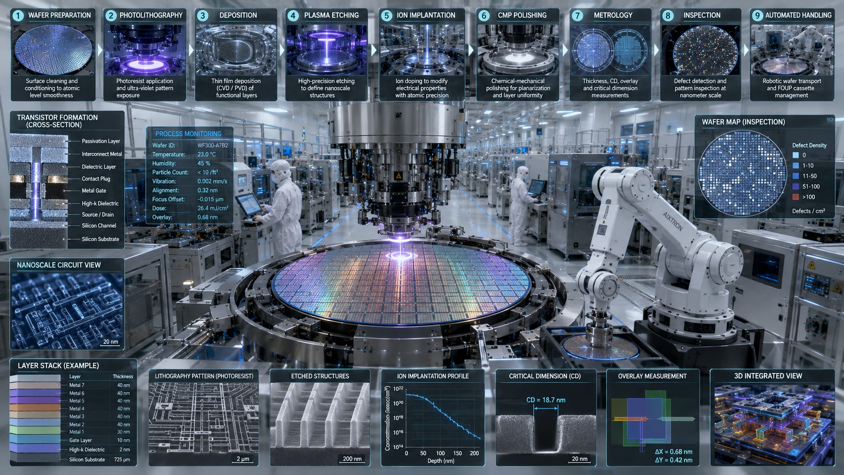
Intel 3 is Intel’s final major FinFET-based process technology (often described as a 3 nm-class node under Intel’s marketing nomenclature), an optimized refinement of the preceding Intel 4 node. It delivers meaningful gains in performance per watt and density while remaining fully within the FinFET transistor architecture, before the company transitions to gate-all-around (RibbonFET) devices and backside power delivery on later nodes such as Intel 18A.
It is not a literal 3 nm physical gate length. Like other modern process names across the industry, “Intel 3” is a marketing designation reflecting overall improvements in power, performance, and area (PPA) rather than a precise dimensional measurement. Intel positions it as competitive in class with TSMC’s N3 family and Samsung’s 3 nm offerings, though architectural and library differences make direct apples-to-apples comparisons imperfect.
Place in Intel’s Process Roadmap
Intel restructured its node naming in 2021 away from traditional nanometer labels (and the earlier “+” enhancement scheme) toward a sequence that better signals generational progress:
- Intel 7 (formerly 10 nm Enhanced SuperFin)
- Intel 4 (first major EUV node, roughly 7 nm-class)
- Intel 3 (refined EUV + FinFET)
- Intel 20A / Intel 18A (RibbonFET GAA + PowerVia backside power, angstrom-era)
- Subsequent nodes such as Intel 14A
Intel 3 reached manufacturing readiness in late 2023 and entered high-volume production in 2024. It serves as a bridge technology: mature enough for high-volume server products and foundry offerings, yet still FinFET-based so that the industry could continue leveraging existing design tools and IP while Intel prepared the more radical architectural shift to GAA.
Core Technical Improvements Over Intel 4
Intel claims the base Intel 3 node delivers up to 18% higher performance at the same power for a full processor core relative to Intel 4, along with up to roughly 8–10% greater logic density. These gains come from a combination of process, device, and design co-optimization rather than a dramatic shrink of every pitch:
- Increased use of extreme ultraviolet (EUV) lithography compared with Intel 4, reducing multi-patterning complexity, mask count, and process variation while improving pattern fidelity.
- Enhanced FinFET transistors with better short-channel effect control, higher intrinsic drive current, and improved contact resistance/capacitance.
- Introduction of denser standard-cell libraries: retention of the 240 nm high-performance (HP) cell height from Intel 4, plus a new 210 nm high-density (HD) library. Designers can mix the two for optimal PPA.
- Optimized interconnect stack with reduced via resistance, lower RC delay, flexible metal-layer counts (options around 14, 18, or 21 layers depending on cost/performance targets), and tighter pitches on selected layers (e.g., M2/M4 improvements).
- Support for a wide voltage range (sub-0.6 V for efficiency up to >1.2–1.3 V for peak performance), enabling both low-power and high-performance applications.
- Dipole work-function metal technology allowing multiple tightly controlled threshold voltages on the same die for better optimization of different circuit blocks.
SRAM bit-cell sizes are reported around 0.024 µm² (high-density) in some disclosures, with further refinements available across variants.
These changes collectively provide what Intel describes as a full-node-class performance uplift in roughly one year—an aggressive pace relative to historical industry norms.
Process Variants for Different Applications
Intel developed a family of related nodes rather than a single monolithic process, reducing risk and expanding market reach:
- Base Intel 3: Core logic process focused on performance and density for compute.
- Intel 3-T: Adds through-silicon vias (TSVs) for 3D stacking applications (HPC, AI, image processing, base dies).
- Intel 3-E: Expands I/O, analog, and mixed-signal capabilities (including native 1.2 V support and deep N-well options), targeting chipsets, storage, and SoC peripherals.
- Intel 3-PT: Combines the above advances with additional performance enhancements, finer-pitch (9 µm) TSVs, and hybrid bonding support for higher-density 3D integration. Positioned as a long-lived “ultimate FinFET” workhorse for both internal products and external foundry customers.
All variants support the 240 nm HP and 210 nm HD libraries. The family is offered through Intel Foundry (with design-services emphasis in some descriptions) alongside internal use.
Products and Real-World Deployment
Intel 3 is primarily a data-center-oriented node. Key products include the Xeon 6 family:
- Sierra Forest (E-core focused, high core-count efficiency designs)
- Granite Rapids (P-core focused, high-performance designs)
These use Intel 3 for the compute dies, often combined with other nodes (e.g., Intel 7 I/O dies) and advanced packaging such as EMIB. Client products have been more limited; some graphics or platform tiles in later hybrid designs have referenced Intel 3, but the primary volume has been server silicon.
The node also supports external foundry customers seeking high-performance logic with mature FinFET tooling.
Comparison Context and Limitations
Versus Intel 4, the gains are clear and quantified by Intel (≈18% performance at iso-power, modest density uplift). Versus later Intel 18A, the differences are larger: 18A introduces RibbonFET GAA transistors and PowerVia backside power delivery, delivering roughly 15–25% higher frequency or 36–38% lower power (depending on voltage and workload) plus ~30% density improvement over Intel 3.
Industry density metrics (transistor density in MTr/mm²) vary by library and design, and public figures for Intel 3 are less aggressive than some TSMC N3 variants in pure logic density. Intel emphasizes performance-per-watt and design flexibility for HPC/server workloads over pure density leadership. SRAM scaling and interconnect efficiency remain important differentiators in real products.
Strategic Role and Longevity
Intel 3 completes the “five nodes in four years” acceleration plan initiated under prior leadership while providing a stable, high-volume platform during the GAA transition. Because it is the last pure FinFET node, design IP, EDA flows, and manufacturing tools remain highly mature. Intel has indicated that variants such as 3-PT will remain relevant for years alongside angstrom-era nodes, especially for cost-sensitive or mixed-signal applications and as a base-die technology in 3D packages.
From a foundry perspective, it expands Intel’s external offerings beyond older nodes and packages, though the company’s strongest competitive push has shifted toward 18A and beyond for leading-edge AI and HPC customers.
Summary of Key Metrics (Intel Claims vs. Prior Node)
| Metric | Intel 3 vs. Intel 4 | Notes |
|---|---|---|
| Performance at iso-power | Up to +18% | Full core |
| Logic density | Up to ~8–10% higher | Via denser HD libraries |
| Cell heights | 240 nm HP + new 210 nm HD | Mixable |
| EUV usage | Increased | Simpler patterning |
| Voltage support | Broad (<0.6 V to >1.2 V) | Flexible |
| Architecture | Enhanced FinFET | Last major FinFET node |
In short, Intel 3 is a pragmatic, high-performance refinement that extracts maximum value from FinFET technology while Intel ramps more revolutionary GAA and backside-power nodes. It underpins current-generation Xeon 6 server CPUs and remains a viable foundry option for designers who prioritize proven FinFET flows, flexible libraries, and strong performance-per-watt characteristics.
1) Core Technical Improvements Over Intel 4
Intel 3 represents a refined, backward-compatible enhancement of the Intel 4 process rather than a full dimensional shrink of every feature. It retains key pitches (contacted poly pitch/CPP at 50 nm, fin pitch near 30 nm, and M0 at 30 nm) while delivering what Intel characterizes as a full-node-class leap in performance and usable density through targeted device, interconnect, and library optimizations. The headline results are up to 18% higher performance at the same power for a full processor core and roughly 8–10% higher logic density.
These gains stem from careful co-optimization across the transistor, contacts, interconnect stack, and standard-cell libraries, combined with greater use of EUV lithography. The improvements are documented primarily from Intel’s 2024 VLSI Symposium disclosures and related technical analyses.
Transistor and Front-End Device Enhancements
The core of the performance uplift lies in better electrostatic control and drive characteristics of the FinFET devices:
- Improved short-channel effects (SCE) — Fin width and profile were optimized. Drain-induced barrier lowering (DIBL) improved by approximately 16 mV/V for NMOS and 27 mV/V for PMOS. Subthreshold slope improved by 5–7 mV/dec relative to Intel 4. These changes yield up to a 5× reduction in off-state leakage at matched drive currents.
- Higher drive current at fixed leakage — Transistors deliver more current for a given leakage target, directly enabling higher frequency at iso-power or lower power at iso-frequency.
- Contact optimization — Fabrication of source/drain contacts was refined to lower both contact resistance and gate-to-contact capacitance. Sharper, more precisely defined contacts further reduce parasitic effects.
- Dipole work-function metal technology — This enables multiple tightly controlled threshold voltages (up to 8 VTs: 4 n-type + 4 p-type spanning a ~200 mV range) on the same die. Unlike traditional thick work-function metals whose volume variations affect threshold, the thin dipole layer induces a controlled charge separation that shifts the effective work function with far better precision and less sensitivity to process variation. This is particularly valuable for foundry customers needing mixed high-performance and low-leakage blocks.
Collectively, these front-end changes produce a reported ~15% higher frequency at matched leakage in ring-oscillator metrics, forming a major part of the overall 18% core-level iso-power gain.
Standard-Cell Library Improvements
Intel 4 primarily offered a 240 nm high-performance (HP) cell height. Intel 3 retains that library while adding a new 210 nm high-density (HD) library:
- The HD library achieves higher transistor density (cell area roughly 10,500 nm² versus 12,000 nm² for the HP library) largely by reducing fin count in many cells (e.g., shifting from 3-fin to 2-fin configurations in places) while preserving the same CPP.
- Designers can mix HP and HD cells within a design for optimal power-performance-area trade-offs. The HD cells also feature a low-resistance wide M0 for better local power delivery.
- Overall logic density improves by up to ~10%, described by Intel as a full-node density step despite the modest pitch scaling.
This dual-library approach gives greater design flexibility than Intel 4, especially for density- or power-sensitive blocks (e.g., efficiency-core clusters in server CPUs).
Interconnect and Back-End Optimizations
Interconnect improvements reduce RC delay and improve routing efficiency without aggressive pitch scaling everywhere:
- Selective pitch tightening — M2 and M4 pitches move from 45 nm (Intel 4) to 42 nm.
- Capacitance reduction — Up to 8% lower capacitance per layer through more extensive direct-print EUV patterning and improved ultra-low-k dielectrics. Barrier and liner optimizations on the lower metal layers (M0–M6) further cut parasitic capacitance.
- Flexible metal-stack options — Designers can choose among cost-oriented (~14 layers), balanced (~18 layers), and high-performance (~21 layers) stacks (exact counts vary slightly by reporting, often expressed as 12+2 / 16+2 / 19+2 including thick global metals). Extra layers improve routing density and reduce congestion.
- Reduced via resistance and overall interconnect RC (both intrinsic and design-enabled) contribute directly to the frequency and power gains.
These back-end changes lower signal delay and power consumption while giving foundry customers more options to balance cost versus performance.
Lithography and Process-Flow Advances
Intel 3 employs more EUV layers than Intel 4. Greater EUV usage simplifies multi-patterning, reduces mask counts in critical layers, improves pattern fidelity, and supports the denser libraries and tighter selected metal pitches with better process control and yield potential.
Supporting Features and Voltage Range
- Broader native voltage support, including 1.2 V I/O transistors and options for deep N-well isolation and long-channel analog devices (especially emphasized in the Intel 3-E variant).
- Maintained or improved SRAM characteristics (high-density cell ~0.024 µm² in some disclosures) with competitive Vmin.
- Compatibility with advanced packaging (Foveros, EMIB) and the addition of TSV/hybrid-bonding options in the 3-T and 3-PT variants.
Quantitative Summary of Key Differences
| Aspect | Intel 4 | Intel 3 | Primary Benefit |
|---|---|---|---|
| Performance (iso-power) | Baseline | Up to +18% (full core) | Frequency or power efficiency |
| Logic density | Baseline (240 nm HP library) | Up to +8–10% (new 210 nm HD + 240 nm HP) | Smaller die or more features |
| Cell heights | 240 nm HP | 240 nm HP + 210 nm HD | Design flexibility |
| DIBL / Subthreshold slope | Baseline | Improved (~16–27 mV/V DIBL, 5–7 mV/dec SS) | Lower leakage, better control |
| Threshold voltage options | Limited | Up to 8 tightly controlled VTs via dipole | Mixed-signal / multi-Vt design |
| Selected metal pitches | M2/M4 ≈ 45 nm | M2/M4 ≈ 42 nm | Lower RC |
| Metal stack flexibility | Primarily ~18 layers | ~14 / 18 / 21 layer options | Cost vs. performance choice |
| EUV intensity | Significant | Increased | Process simplification, fidelity |
In practice, these refinements allowed Intel to ship high-volume Xeon 6 processors (Sierra Forest and Granite Rapids) on Intel 3 while positioning the node family as a long-lived FinFET platform for both internal products and external foundry customers. The improvements demonstrate that substantial PPA gains remain achievable even late in the FinFET era through continuous device and interconnect engineering rather than pure geometric scaling alone.
Process Variants of Intel 3 for Different Applications
Intel developed Intel 3 not as a single monolithic process but as a family of closely related variants. These were co-architected and incrementally refined to reduce risk, accelerate time-to-market, and address a wider range of product needs—from high-performance compute dies to analog-heavy chipsets and advanced 3D-stacked systems. All variants share the same foundational FinFET technology, 240 nm high-performance and 210 nm high-density standard-cell libraries, and the core performance and density gains versus Intel 4. Differences appear primarily in packaging features, I/O and analog capabilities, and design ease-of-use options.
This modular approach allows Intel (and external foundry customers) to select the most appropriate flavor without redesigning the entire process flow from scratch.
Base Intel 3
The foundational node focuses on pure logic performance and density for general-purpose compute.
- Optimized for high-performance processor cores and logic-heavy tiles.
- Delivers the full claimed up to 18% performance uplift at iso-power and ~8–10% density improvement over Intel 4.
- Flexible metal interconnect stacks (cost-oriented, balanced, or high-performance layer counts).
- Supports the full range of voltages from low-power operation below 0.6 V up to high-performance regimes above 1.2 V.
- Primary internal use: compute dies in data-center processors.
- Suitable for server, client, and base-die applications where advanced stacking or rich analog features are not required.
This is the workhorse version used in high-volume manufacturing for products such as the Xeon 6 family compute tiles.
Intel 3-T
Builds directly on the base process by adding through-silicon vias (TSVs) optimized for 3D integration.
- Enables vertical stacking of multiple dies (compute + memory, or multiple compute layers) within a single package.
- Targets applications that benefit from high-bandwidth, low-latency interconnect between stacked components—high-performance computing (HPC), AI accelerators, image sensors/processors, and dense multi-chip modules.
- Supports standard TSV pitches suitable for Foveros-style or similar advanced packaging flows.
- Maintains the same performance and density characteristics as the base node while adding the vertical connectivity needed for disaggregated or stacked architectures.
- Useful as a base die in multi-tile packages where power delivery or signal routing must pass through the silicon.
This variant is particularly relevant for systems that combine logic with high-bandwidth memory or other specialized tiles in a 3D configuration.
Intel 3-E
Extends the base process with a richer set of I/O, analog, and mixed-signal features.
- Native support for 1.2 V operation, long-channel devices, and deep N-well isolation.
- Enhanced analog and mixed-signal capabilities that make it suitable for peripheral controllers, platform controller hubs (PCH-like functions), storage controllers, and other SoC blocks that require more than pure high-speed digital logic.
- Broader design library support for external interfaces and lower-speed, higher-voltage circuits.
- Targets chipset, storage, networking, and mixed-signal markets where pure compute performance is secondary to integration of analog functions and robust I/O.
- Still retains the core logic performance improvements, allowing hybrid designs that combine digital and analog domains on the same die or tile.
This flavor expands the addressable market beyond pure CPU cores into more complete system-on-chip or companion-chip applications.
Intel 3-PT
The most comprehensive and highest-capability member of the family. It combines the features of the preceding variants and adds further enhancements.
- Incorporates the performance and density of the base node, the TSV capabilities of 3-T, and the expanded I/O/analog features of 3-E.
- Adds finer-pitch 9 µm TSVs and support for hybrid bonding, enabling denser and higher-bandwidth 3D stacking than the standard 3-T option.
- Includes additional performance-oriented process tweaks and superior ease-of-use features for designers (improved design rules or library support that simplify implementation).
- Positioned by Intel as the “ultimate FinFET” node—a long-lived platform expected to remain relevant for both internal products and external foundry customers alongside future GAA nodes.
- Ideal for complex, high-value applications that need the best combination of logic performance, 3D integration density, analog flexibility, and design productivity (advanced AI/HPC packages, high-end custom silicon, and multi-die systems).
Intel has indicated that 3-PT will serve as a mainstay technology for years, especially where the maturity and cost structure of FinFET remain advantageous compared with newer RibbonFET processes.
Summary Comparison of Variants
| Variant | Key Additions | Primary Target Applications | Notable Features |
|---|---|---|---|
| Base Intel 3 | Core logic performance & density | Server/client compute dies, general logic | Full 18% iso-power gain, flexible metal stacks |
| Intel 3-T | Through-silicon vias (TSVs) | 3D stacking, HPC, AI, base dies | Vertical interconnect for multi-die packages |
| Intel 3-E | Expanded I/O, analog, mixed-signal | Chipsets, storage, SoC peripherals | 1.2 V native, deep N-well, long-channel devices |
| Intel 3-PT | All of the above + finer TSVs & hybrid bonding + extra performance/ease-of-use | Advanced 3D systems, high-end custom silicon, long-term foundry use | 9 µm pitch TSVs, hybrid bonding, highest overall capability |
Strategic Value of the Variant Approach
By offering this family, Intel reduces risk—each variant can be qualified and ramped independently while sharing the majority of the process flow and design infrastructure. Customers (internal product teams or external foundry clients) can match the process to the exact needs of their product without paying for unused features. The approach also extends the commercial life of FinFET technology: even after Intel transitions leading-edge volume to RibbonFET nodes such as 18A, the mature Intel 3 family (especially 3-PT) remains available for cost-sensitive, mixed-signal, or high-volume applications that do not require the absolute densest or lowest-power transistors.
In practice, the base and 3-T variants have seen the earliest high-volume deployment in Xeon 6 processors, while 3-E and 3-PT expand the foundry and specialized-product opportunities. Together they illustrate how a late-stage FinFET platform can still deliver meaningful differentiation across a broad set of real-world applications.
Products and Real-World Deployment of the Intel 3 Process Node
Intel 3 entered high-volume manufacturing in 2024 and remains a production workhorse in 2026, primarily powering data-center CPUs while also serving secondary roles in client tiles, base dies for newer multi-chiplet packages, and Intel Foundry offerings. Its real-world deployment centers on the Xeon 6 family, with continued capacity expansion and ongoing use alongside the newer Intel 18A node.
Primary Products: Xeon 6 Server Processors
The flagship deployment of Intel 3 is the Xeon 6 series, Intel’s sixth-generation scalable server platform. Compute dies are fabricated on Intel 3, while I/O dies typically use the more mature Intel 7 process and are connected via EMIB packaging.
- Sierra Forest (Xeon 6 E-core variants) — Launched in June 2024 (initial 6700E series with up to 144 cores; higher-core-count 6900E configurations followed). These all-E-core designs (Sierra Glen / Crestmont-derived architecture) target high-density, power-efficient cloud-native, microservices, and scale-out workloads. Core counts reach 144–288 depending on configuration. They delivered strong performance-per-watt gains and saw rapid adoption in telecommunications (5G core, vRAN) and hyperscale environments.
- Granite Rapids (Xeon 6 P-core variants) — Launched later in 2024 (6900P series with up to 128 P-cores initially, followed by broader 6700P/6500P/6300P SKUs). These use Redwood Cove P-cores on Intel 3 compute tiles and emphasize higher single-thread and AI/HPC performance. Configurations support multi-socket platforms, high memory bandwidth (DDR5, including MRDIMM options in some SKUs), and extensive PCIe/CXL connectivity. They serve traditional enterprise, virtualization, database, and AI-inference workloads.
Both families use a multi-tile architecture: Intel 3 for the high-performance compute silicon and Intel 7 for I/O and memory controllers. This disaggregation improves yields and allows independent scaling of cores versus I/O.
Continued Role in Newer Multi-Chiplet Designs
Even after the introduction of Intel 18A, Intel 3 remains relevant as a base-die or companion technology:
- In Xeon 6+ Clearwater Forest (launched 2026, up to 288 E-cores on 18A compute tiles), the active base tiles that hold large L3 cache and memory logic are fabricated on Intel 3. This hybrid approach leverages the maturity and density characteristics of Intel 3 for non-compute functions while placing the newest RibbonFET cores on 18A.
- Future Xeon 7 (Diamond Rapids, targeted around 2027) is expected to use advanced 18A variants for compute tiles, with reports indicating Intel 3 may still appear in I/O or supporting tiles in multi-chiplet packages.
Client and Other Internal Uses
Client deployment of pure Intel 3 compute is limited compared with servers, as Intel shifted many client products toward external foundries or later internal nodes. However:
- Certain graphics tiles in Panther Lake (Core Ultra Series 3, 18A compute) use Intel 3 for the smaller 4-Xe configurations.
- Some Intel Core Ultra Series 2 variants referenced Intel 3 manufacturing depending on specific SKUs.
- Platform controller or secondary tiles in hybrid designs have utilized the node.
Overall, client volume on Intel 3 has been secondary to its data-center focus.
Foundry and External Deployment
Intel positioned Intel 3 as its first leading-edge foundry node available to external customers, with production at both Oregon (R&D/high-volume) and Leixlip, Ireland facilities. Design wins were announced across Intel 3 (alongside Intel 16 and packaging services), and the node family (including 3-T, 3-E, and 3-PT variants) is offered for high-performance compute, 3D stacking, and mixed-signal applications.
Public details on specific external customer products remain limited compared with internal Xeon volume, but the node supports design services and is intended as a long-lived FinFET platform for third-party HPC, AI, networking, and custom silicon. Capacity investments (including a significant expansion at the Ireland site) continue to support both internal Xeon production and external demand.
Production Status and Capacity as of 2026
- High-volume manufacturing began in late 2023/early 2024 at Oregon and Ireland fabs.
- Xeon 6 processors based on Intel 3 have been shipping in volume since mid-to-late 2024 and remain in active production and deployment through 2026.
- Intel continues to invest in capacity (e.g., multi-billion-euro expansions at Leixlip) specifically to scale Intel 3 output for ongoing Xeon 6 demand and supporting roles in next-generation packages.
- The node coexists with Intel 18A (now in high-volume for Panther Lake client and Clearwater Forest server products). Intel 3 serves as a mature, cost-effective complement rather than being fully displaced.
Real-World Impact and Adoption Notes
Xeon 6 on Intel 3 enabled measurable efficiency gains in data centers and telecom networks, with partners reporting substantial improvements in performance per watt and rack density for cloud, 5G, and enterprise workloads. The multi-tile design and process maturity contributed to better yields and supply availability relative to earlier leading-edge transitions.
In summary, Intel 3’s primary real-world success is the Xeon 6 platform, which established it as a high-volume server workhorse. Its secondary roles as base dies in 18A packages and as a foundry offering extend its commercial life well into the angstrom era, demonstrating the value of a refined, production-proven FinFET technology even as the industry moves to gate-all-around transistors.