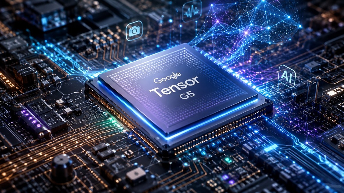
Tensor G5 is Google’s fifth-generation mobile SoC and the most significant redesign in the series. It prioritizes on-device AI, imaging, efficiency, and everyday responsiveness over pure peak synthetic performance. Unlike rivals focused on maximum multi-core or graphics horsepower, Google optimizes Tensor around software-hardware co-design with Gemini Nano, computational photography, and proactive features that run privately on-device.
Manufacturing Shift: From Samsung to TSMC 3nm
Previous Tensor chips (G1 through G4) relied on Samsung Foundry processes (primarily 5nm and 4nm nodes). These delivered solid AI and imaging results but lagged in power efficiency and sustained performance due to process maturity and thermal constraints.
Tensor G5 moves production to TSMC’s advanced 3nm process (widely reported as N3E). This change enables higher transistor density, better power efficiency, higher clock speeds on familiar Arm cores, and improved thermal headroom. Google states the node allows packing more transistors for greater power and efficiency. Early real-world feedback and battery claims (Pixel 10 series advertised at 30+ hours versus ~24+ on Pixel 9) align with meaningful efficiency gains, though larger batteries and other system optimizations also contribute.
This is the first Tensor built without Samsung as the primary foundry partner. Google retained some custom blocks (TPU, DSP, memory compressor, audio processor) while licensing third-party IP for other functions to complete the design.
CPU Architecture and Performance
Tensor G5 uses an octa-core Arm configuration rearranged for better multi-threaded balance:
- 1× Cortex-X4 prime core at up to 3.78 GHz
- 5× Cortex-A725 mid-cores at up to 3.05 GHz
- 2× Cortex-A520 efficiency cores at up to 2.25 GHz
Compare this with Tensor G4’s 1× X4 (3.1 GHz) + 3× A720 (2.6 GHz) + 4× A520 (1.92 GHz). The shift from a 1+3+4 to a 1+5+2 layout increases mid-core count for sustained multi-threaded work while the process node and higher clocks deliver single-core gains. Google claims an average 34% faster CPU than Tensor G4.
Independent benchmarks generally support solid generational uplift:
- Geekbench 6 single-core: roughly 2,200–2,350 (Pixel 10 Pro models often at the higher end)
- Geekbench 6 multi-core: roughly 6,000–6,500
- AnTuTu overall scores typically fall in the 1.2–1.5 million range depending on device and test conditions
These figures place Tensor G5 ahead of G4 (often ~20–40% multi-core gains) but still behind contemporary flagships such as Snapdragon 8 Elite or Apple A18/A19-class chips in raw multi-core and peak throughput. The design philosophy favors balanced, efficient everyday performance and thermal stability over chasing leaderboard numbers.
GPU: Switch to Imagination Technologies PowerVR
Tensor G5 replaces the previous Arm Mali graphics with an Imagination Technologies PowerVR DXT-48-1536 (clocked around 1.1 GHz in reports). This is a notable architectural change. The DXT series uses Imagination’s Photon architecture.
Graphics performance shows mixed results versus Tensor G4’s Mali-G715. Some synthetic tests indicate modest gains or even slight regressions in certain scenarios, while real-world gaming and sustained performance benefit from the process node’s efficiency. Ray tracing support is absent. Google has historically under-emphasized high-end gaming relative to competitors; Tensor G5 continues that pattern while still delivering playable performance for most titles.
Third-party IP also appears in the display controller (VeriSilicon DC9000) and video codec (Chips&Media WAVE677DV supporting AV1, VP9, HEVC, and H.264 up to 4K120). Google dropped its earlier custom “BigWave” AV1 block in favor of the off-the-shelf solution.
Tensor Processing Unit (TPU) and On-Device AI
The standout upgrade is the fourth-generation TPU, claimed to be up to 60% more powerful than the prior generation. This is where Google’s silicon strategy shines. Tensor G5 is the first chip designed to run the newest Gemini Nano model fully on-device at launch.
Key AI claims and capabilities:
- Gemini Nano runs approximately 2.6× faster and 2× more efficiently for tasks such as Pixel Screenshots and Recorder
- Support for larger models and longer context (reports of up to 32,000 tokens)
- Architectural techniques including Matryoshka Transformer and per-layer embeddings that allow dynamic scaling of parameters without excessive memory pressure
- New proactive features such as Magic Cue, Voice Translate (preserving speaker voice), Call Notes with actions, Personal Journal, enhanced Scam Detection, and improved Gboard voice editing
All of these operate on-device for privacy and low latency. The TPU works in concert with the improved ISP and DSP to enable advanced computational photography, including higher-quality real-time diffusion models for zoom and editing.
Imaging and Other Subsystems
Google continues refining its custom Image Signal Processor. The G5 generation features a more fully Google-designed ISP that improves motion deblur, scene segmentation, Real Tone accuracy, and enables features such as 100× ProRes Zoom on Pro models and better 10-bit video capture. Camera performance remains a Pixel strength, with the silicon tightly integrated into the software pipeline.
Memory support is LPDDR5X; storage moves toward UFS 4.0 (especially on higher capacities). Connectivity includes a Samsung Exynos 5400 5G modem in many reports, Wi-Fi 7, and Bluetooth 6.0. Enhanced security hardware protects the device from manufacturing through daily use.
How Tensor G5 Compares to Competitors and Prior Generations
| Aspect | Tensor G5 | Tensor G4 | Typical Flagship (e.g., Snapdragon 8 Elite) |
|---|---|---|---|
| Process | TSMC 3nm | Samsung 4nm | TSMC 3nm |
| CPU Layout | 1× X4 + 5× A725 + 2× A520 | 1× X4 + 3× A720 + 4× A520 | More aggressive prime/mid clusters |
| Claimed CPU Gain | +34% average vs G4 | — | Higher peak multi-core |
| TPU/NPU Focus | +60% claimed, Gemini Nano optimized | Strong but lower throughput | Strong general NPU, less Google-specific |
| GPU | PowerVR DXT-48-1536 | Arm Mali-G715 | Adreno with ray tracing |
| Design Philosophy | AI, imaging, efficiency, privacy | AI & imaging | Peak performance & gaming |
Tensor G5 closes the efficiency gap with leading chips while widening Google’s lead in tightly integrated on-device generative AI and photography. It does not attempt to match the absolute highest synthetic scores; instead it delivers responsive daily use, longer sustained performance under AI and camera loads, and exclusive Pixel experiences.
Real-World Implications and Limitations
Users of Pixel 10 series devices experience snappier everyday tasks, more capable offline AI assistants, superior computational photography, and improved battery life relative to prior Pixels. Thermal behavior benefits from the 3nm process, reducing throttling in prolonged workloads.
Limitations remain consistent with Google’s approach: gaming and pure multi-core productivity trail the absolute flagships, and some third-party IP choices (GPU, modem) mean Google does not control every aspect of the silicon. Future generations will likely continue refining the custom blocks while leveraging TSMC process advances.
In summary, Tensor G5 marks the transition of Google’s mobile silicon from an ambitious but process-constrained design into a more mature, efficiency-focused platform optimized for the AI-first smartphone era. It is not the fastest chip on paper, but it is the one most tightly aligned with Google’s vision of private, proactive, on-device intelligence.
Google Tensor G5 CPU Architecture
Core Configuration and Cluster Layout
Tensor G5 employs a classic hybrid (prime / big.LITTLE-style) octa-core design using licensed Arm Cortex cores under the ARMv9.2-A instruction set. The specific arrangement is a 1+5+2 configuration:
- 1× Cortex-X4 (prime / performance core) clocked at up to 3.78 GHz
- 5× Cortex-A725 (mid / performance cores) clocked at up to 3.05 GHz
- 2× Cortex-A520 (efficiency / little cores) clocked at up to 2.25 GHz
This is a deliberate evolution from Tensor G4’s 1+3+4 layout (1× Cortex-X4 at 3.1 GHz + 3× Cortex-A720 at 2.6 GHz + 4× Cortex-A520 at ~1.92–1.95 GHz). Google increased the number of mid-cores while reducing the little-core count and leveraged the TSMC 3 nm (N3E) process to raise clocks substantially across the board.
Design rationale behind the 1+5+2 shift:
- More mid-cores improve multi-threaded throughput for everyday multitasking, app switching, background AI tasks, and sustained workloads without relying heavily on the power-hungry prime core.
- Fewer little cores reduce overhead while the higher clocks and better process node still deliver strong efficiency for light tasks.
- The single high-clocked X4 prioritizes responsive single-threaded performance (app launches, UI fluidity, browser rendering).
Google claims an average ~34% CPU performance uplift versus Tensor G4. Independent Geekbench 6 results typically show single-core scores in the 2,200–2,350 range and multi-core scores around 6,000–6,500, confirming meaningful generational gains—especially in multi-core scenarios—while remaining behind pure flagship competitors that use newer Arm cores or custom designs.
Individual Core Characteristics
Cortex-X4 (Prime Core)
Arm’s high-performance core from the 2023 generation (still current for many mid-to-high designs in 2025). It features a wide out-of-order execution engine, large caches, and strong single-thread IPC (instructions per clock). The jump from 3.1 GHz on Samsung 4 nm to 3.78 GHz on TSMC 3 nm is one of the most visible benefits of the foundry switch, delivering clear single-core responsiveness gains.
Cortex-A725 (Mid Cores)
These are the updated mid-range cores (successor lineage to A720). They offer a strong balance of performance and efficiency, with improved IPC over the previous A720 generation. Deploying five of them is the architectural highlight: it creates a broad “performance middle” that handles the majority of concurrent tasks efficiently, reducing the need to wake the X4 as frequently and improving sustained performance under thermal constraints.
Cortex-A520 (Efficiency Cores)
The little cores focus on ultra-low power for background processes, always-on sensing, and light system tasks. Reducing them from four to two, while raising clocks, still provides adequate efficiency headroom thanks to the superior process node.
All cores support modern Arm features including pointer authentication, memory tagging, and other ARMv9 security and reliability extensions that Google leverages for Pixel’s security model.
Cache Hierarchy and Memory Subsystem Support
Public specifications list an 8 MB L3 / system-level cache (SLC). Per-core private caches follow typical Arm patterns (approximate figures from detailed teardowns and database entries):
- L1: ~64 KB instruction + 64 KB data on the X4 and A725 cores; smaller (~16 KB) on A520
- L2: Larger private L2 on the prime core (around 1 MB), shared or per-core L2 on mid-cores (hundreds of KB), smaller on efficiency cores
The memory subsystem pairs with LPDDR5X (up to ~4.266 GHz / 8533 MT/s in some reports), delivering bandwidth on the order of 68 GB/s. This supports the wider mid-core cluster and the demanding TPU/ISP workloads without becoming a frequent bottleneck.
Process Node Impact and Efficiency Philosophy
Manufacturing on TSMC’s 3 nm node (versus Samsung’s 4 nm for G4) is foundational. Higher transistor density and better power characteristics enable the elevated clocks without proportional power or thermal penalties. Real-world effects include:
- Better sustained multi-core performance under prolonged loads (less aggressive throttling)
- Improved battery life contribution for CPU-bound tasks
- Greater thermal headroom for concurrent AI + camera + UI workloads
Google’s overall philosophy remains distinct from Qualcomm or MediaTek flagship approaches. Tensor G5 does not chase the absolute newest Arm cores (e.g., no Cortex-X925) or maximal core counts for synthetic leadership. Instead, it prioritizes a balanced, efficient configuration tightly co-designed with Google’s software stack, Gemini Nano on-device inference, and computational photography pipeline.
Comparison Snapshot: Tensor G5 vs Tensor G4 vs Typical Flagship
| Aspect | Tensor G5 | Tensor G4 | Typical 2025 Flagship (e.g., Snapdragon 8 Elite class) |
|---|---|---|---|
| Process | TSMC 3 nm | Samsung 4 nm | TSMC 3 nm |
| Cluster Layout | 1× X4 + 5× A725 + 2× A520 | 1× X4 + 3× A720 + 4× A520 | Often 1–2 primes + more aggressive mid/little mixes |
| Peak Clocks | 3.78 / 3.05 / 2.25 GHz | 3.1 / 2.6 / ~1.95 GHz | Frequently higher or with newer microarchitectures |
| Focus | Balanced multi-thread + efficiency | Similar, less mid-core emphasis | Peak single- and multi-core leadership |
| Cache (L3/SLC) | 8 MB | Similar range | Varies; often competitive |
Implications for Real-World Use
The architecture delivers noticeably snappier everyday responsiveness and stronger multi-tasking than previous Pixels. It shines in scenarios involving concurrent AI features (on-device Gemini Nano), camera processing, and light-to-moderate productivity. Gaming and heavy multi-core content creation still trail the absolute highest-end chips, consistent with Google’s long-standing priority ranking of AI, photography, and software experience over raw benchmarks.
In short, Tensor G5’s CPU is an evolutionary but strategically refined design: familiar Arm cores, cleverly rebalanced clusters, elevated clocks enabled by TSMC 3 nm, and a clear focus on efficient, sustained performance that serves Pixel’s unique software strengths. It is not the fastest CPU in the Android flagship arena, but it is one of the most purposefully optimized for the tasks Google considers most important.
GPU capabilities
Architecture and Core Specifications
Tensor G5 replaces the long-standing Arm Mali GPUs (used from Tensor G1 through G4) with an Imagination Technologies PowerVR DXT-48-1536 (also referred to as IMG DXT-48-1536). This is based on Imagination’s Photon architecture from the D-Series (introduced around 2023).
Key hardware specifications:
- Configuration: DXT-48-1536 — 48 pixels per clock, with 1,536 FP32 FLOPs per clock cycle
- Pipelines / Compute Units: 6
- Shading Units: 128 per unit → total of 768 shaders
- Clock Speed: Up to 1.1 GHz (1,100 MHz)
- Theoretical Performance: Approximately 1.69 TFLOPS FP32 (and roughly double that for FP16)
- Process Node: Manufactured as part of the TSMC 3 nm (N3E) SoC, which aids efficiency
The “48-1536” naming convention indicates fill rate and compute density. Imagination designed the DXT series for better scalability and granularity than its prior CXT generation, with improvements in Universal Shader Clusters (USC) delivering higher compute and texture performance per unit.
Feature Support and Capabilities
API and Software Support:
- Vulkan 1.4 (full conformity confirmed; early software had incomplete driver support that Google later addressed via updates)
- OpenCL 3.0 (FP)
- OpenGL ES 3.x / 2.0 / 1.1 + extensions
- Android NN HAL support (for neural network acceleration offload)
- DirectX 12.0 compatibility in some listings
Key Hardware Features:
- Fragment shading rate
- 2D dual-rate texturing
- Pipelined data masters
- RISC-V firmware
- ASTC HDR texture support
- Advanced framebuffer compression (PVRIC5)
- Support for modern texture formats (PVRTC, ETC, ASTC)
Ray Tracing: The underlying DXT architecture supports scalable ray tracing (via optional Ray Acceleration Clusters). However, Google explicitly chose a non-ray-tracing configuration for Tensor G5. There is no hardware ray tracing enabled (confirmed by Google and independent analysis). This is a deliberate omission—likely for die area, power, or cost reasons—consistent with Pixel’s historical de-emphasis on high-end gaming features.
GPU Virtualization: The DXT design supports HyperLane-style virtualization, allowing accelerated graphics in virtual machines. This aligns with Google’s broader interest in virtualization features on Pixel devices.
Video and Multimedia Integration: While the primary video codec block is a separate third-party solution (Chips&Media WAVE677DV), the GPU contributes to overall graphics and compute workloads that feed into the imaging and display pipeline.
Performance Characteristics
Google was relatively quiet on GPU gains, stating only that graphics were “improved.” Real-world and synthetic results show a nuanced picture:
- Peak performance: In 3DMark Wild Life Extreme, Tensor G5 delivered roughly a 27% peak improvement over Tensor G4 in some tests, with notably better stability (less aggressive thermal throttling—e.g., ~89% vs ~80% stability scores).
- AnTuTu GPU scores: Often mixed or even slightly lower than Tensor G4’s Mali-G715 MP7 in early tests (e.g., ~380k–416k vs higher Mali scores), though overall system scores rose due to strong CPU and efficiency gains.
- Sustained performance: The TSMC 3 nm process and new architecture generally provide better thermal consistency than prior Samsung-built Tensors. Gaming sessions show smoother long-term frame rates with less jitter once drivers matured.
- Early software limitations: At launch, incomplete drivers (stuck at lower Vulkan levels or under-clocked in some scenarios) caused underwhelming results. Subsequent updates (including Android 16 QPR updates) significantly improved driver maturity, unlocking better performance and full Vulkan 1.4 support.
Overall, the GPU sits in the mid-to-upper mid-range for 2025 flagships—competitive with mid-high Adreno or Mali configurations but clearly behind Snapdragon 8 Elite-class Adreno GPUs or Apple’s high-end designs in raw throughput and advanced gaming features.
Comparison Snapshot
| Aspect | Tensor G5 (PowerVR DXT-48-1536) | Tensor G4 (Arm Mali-G715 MP7) | Typical Flagship (e.g., Snapdragon 8 Elite Adreno) |
|---|---|---|---|
| Architecture | Imagination Photon (D-Series) | Arm Valhall 4th gen | Custom Adreno |
| Peak Clock | 1.1 GHz | ~940 MHz | Higher (often 1 GHz+) |
| Theoretical FP32 | ~1.69 TFLOPS | ~1.68 TFLOPS | Significantly higher |
| Ray Tracing | Not enabled | Not supported | Supported |
| Vulkan | 1.4 | 1.3 | 1.3/1.4 |
| Focus | Efficiency + stability | Solid mid-range | Peak gaming & compute |
| Sustained Performance | Improved thermal consistency | More throttling-prone | Strong |
Design Philosophy and Real-World Implications
Google’s switch to Imagination was driven by the move to a fully independent TSMC-based design (ending reliance on Samsung IP blocks). The DXT GPU prioritizes power efficiency, modern API support, and features useful for Pixel’s software ecosystem (UI smoothness, AR, computational photography assists, and potential virtualization) over chasing maximum gaming FPS or ray-traced visuals.
Strengths:
- Better sustained performance and thermal behavior than prior Tensors
- Modern API support (especially post-driver updates)
- Efficiency gains from the 3 nm process
- Adequate for most games at high settings with good consistency
Limitations:
- No ray tracing
- Peak graphics horsepower lags true 2025 flagships
- Early software optimization issues (largely mitigated by updates)
- Pixel remains a secondary choice for hardcore mobile gamers
In practice, casual and mid-tier gaming (Call of Duty Mobile, Genshin Impact at moderate settings, emulators, etc.) runs smoothly. Demanding titles or prolonged high-refresh sessions still reveal the gap versus leading Adreno implementations. For the majority of Pixel users—who prioritize photography, AI features, software experience, and battery life—the GPU is more than sufficient and benefits from the overall system efficiency improvements.
The Tensor G5 GPU represents a pragmatic, efficiency-oriented choice that completes Google’s transition to a more independent silicon platform. It is not a graphics powerhouse, but it is a capable, modern, and better-behaved engine that aligns with Pixel’s core strengths.
Tensor Processing Unit (TPU) and On-Device AI in Google Tensor G5
The core question is a request for a detailed technical explanation of the Tensor Processing Unit (TPU) in the Google Tensor G5 SoC, along with how it enables and advances on-device AI capabilities—particularly the integration with Gemini Nano, architectural innovations, performance gains, real-world features, privacy/efficiency benefits, and comparisons to prior generations. This is the true centerpiece of Google’s Tensor strategy: a custom neural engine purpose-built for the AI workloads that define the Pixel experience.
What Is the Tensor Processing Unit (TPU)?
In the mobile context, Google’s TPU (sometimes called Edge TPU) is a dedicated neural processing unit (NPU) optimized for machine learning inference. Unlike general-purpose CPU or GPU cores, it is specialized for the matrix multiplications, convolutions, and transformer operations that dominate modern AI models—especially language models, vision models, and speech processing.
On Tensor G5, this is the fourth-generation TPU. Google claims it delivers up to 60% more power than the third-generation TPU in Tensor G4. The gains come from a combination of additional compute blocks, higher operating frequency, architectural refinements, and the efficiency of the TSMC 3 nm process node.
The TPU works in close coordination with the CPU, DSP, and ISP. Heavy AI tasks are offloaded to the TPU for speed and power efficiency, while the rest of the SoC handles supporting work (data movement, post-processing, UI responsiveness).
Key Architectural and Software Innovations
Google co-designed the G5 TPU with DeepMind specifically around the newest Gemini Nano model. Two important techniques stand out:
- Matryoshka (or Matformer) Transformer Architecture
- This embeds smaller sub-models inside a larger parent model. Applications can dynamically choose speed versus quality by activating different “layers” of the nested structure. It allows a single model binary to serve both lightweight and higher-quality use cases without loading entirely separate models.
- Per-Layer Embedding (PLE)
- Model parameters are not all kept in RAM. Instead, they reside primarily in flash storage and are paged into memory in tiny increments as needed. This dramatically reduces the DRAM footprint. Example figures reported: the full Gemini Nano model can have ~8 billion parameters, but only a subset (e.g., 2–4 billion effective parameters) needs to reside in RAM at any moment. This is critical on mobile devices with limited memory budgets.
These techniques, combined with the stronger TPU, allow Gemini Nano to run 2.6× faster and 2× more efficiently (in energy terms) for key workloads such as Pixel Screenshots and the Recorder app compared with Tensor G4.
Context window has also expanded significantly—from roughly 12,000 tokens on G4-era devices to up to 32,000 tokens on G5. This is equivalent to processing roughly a month of emails or around 100 screenshots in a single on-device context, enabling richer multi-turn and multi-modal reasoning without cloud round-trips.
Performance and Efficiency Gains
Google’s headline numbers for the TPU:
- Up to 60% higher computational throughput versus the prior generation.
- Gemini Nano inference: 2.6× faster and 2× more power-efficient for representative tasks.
- Support for larger, higher-quality models that previously would have required cloud offload or significant compromises.
Independent synthetic AI benchmarks (Geekbench AI, AI Benchmark, etc.) have shown mixed results depending on the backend used (NNAPI vs. proprietary paths) and memory configuration. Devices with 16 GB RAM (Pro models) generally fare better than the 12 GB base models, as memory bandwidth and capacity remain limiting factors for large model inference. Google prioritizes its own tightly optimized paths over generic Android NNAPI scores, so third-party benchmarks do not always fully reflect the real-world gains users experience inside Pixel software.
The move to TSMC 3 nm further improves sustained AI performance by reducing thermal throttling and power draw under prolonged inference loads.
On-Device AI Features Powered by the G5 TPU
Tensor G5 + Gemini Nano unlocks or significantly improves more than 20 on-device generative AI experiences at launch. Key examples include:
- Magic Cue — Proactive, context-aware suggestions that surface relevant information (calendar, messages, notes) without explicit queries.
- Voice Translate — Real-time call translation that preserves the speaker’s own voice characteristics.
- Call Notes with actions — Automatic summarization of calls plus suggested follow-up actions.
- Personal Journal — On-device journaling assistance and insight generation.
- Enhanced Pixel Screenshots and Recorder — Faster, higher-quality summarization and transcription.
- Scam Detection and improved Gboard voice editing / natural language features.
- Advanced computational photography models (including large diffusion models for zoom and editing) that run with lower latency and better quality.
All of these run fully or primarily on-device, delivering low latency, offline functionality, and strong privacy (sensitive data never leaves the device).
Privacy, Latency, and Offline Advantages
On-device AI is central to Google’s Pixel differentiation:
- Privacy — Personal data (conversations, photos, screenshots, journal entries) stays local.
- Latency — No network round-trip means near-instant responses for many features.
- Reliability — Features continue working in airplane mode or poor connectivity.
- Cost and scalability — No per-inference cloud charges for the user or Google.
The TPU is purpose-built so that these benefits can be delivered without sacrificing model quality.
Comparison: Tensor G5 TPU vs. Prior Generations and Competitors
| Aspect | Tensor G5 (4th-gen TPU) | Tensor G4 (3rd-gen TPU) | Typical Flagship NPU (e.g., Snapdragon Hexagon) |
|---|---|---|---|
| Claimed Performance Uplift | Up to +60% | Baseline | Competitive general NPU |
| Gemini Nano Support | Newest model, fully on-device | Previous generation | Limited / different model |
| Inference Speed (example) | 2.6× faster on key tasks | Baseline | Varies by model |
| Efficiency | 2× better energy use on key tasks | Baseline | Strong |
| Context Window | Up to 32K tokens | ~12K tokens | Varies |
| Design Focus | Deep integration with Gemini Nano & Pixel features | Strong but more constrained | Broad developer ecosystem |
Google does not compete on open TOPS leaderboards the way some rivals do. Instead, it optimizes the TPU + software stack specifically for the models and features it ships. This produces excellent results inside the Pixel ecosystem while remaining less flexible for third-party developers who want to run arbitrary large models.
Limitations and Real-World Context
- Memory remains a constraint; base models with 12 GB RAM dedicate a significant portion to always-resident AI models, reducing free RAM for apps.
- Third-party AI frameworks may not fully leverage the TPU without Google-specific plugins, so generic benchmarks can understate capability.
- While the TPU is the strongest part of Tensor G5 relative to its predecessors, absolute peak AI throughput still trails the most aggressive competitors in some synthetic tests.
Summary: Why the TPU Defines Tensor G5
The fourth-generation TPU is the heart of Tensor G5’s value proposition. Combined with Matryoshka/Matformer techniques, Per-Layer Embedding, a larger context window, and deep co-design with Gemini Nano, it delivers faster, more efficient, higher-quality on-device generative AI than any previous Pixel generation. Features that once required cloud connectivity or significant compromises now run privately and responsively on the device itself.
In Google’s hierarchy of priorities, the TPU outranks raw CPU or GPU leadership. Tensor G5 is not designed to win synthetic multi-core or gaming benchmarks; it is designed to make advanced AI feel instantaneous, private, and battery-friendly in everyday Pixel use. That focus is what makes the TPU—and the on-device AI it enables—the most important upgrade in the Tensor G5 platform.
Image Signal Processor
What an ISP Does and Why It Matters on Pixel
An Image Signal Processor handles the complex, real-time conversion of raw Bayer (or other) sensor data into usable images and video. Core tasks include demosaicing, noise reduction, white balance, color correction, tone mapping, sharpening, HDR merging, and motion compensation. On modern smartphones—particularly Pixels—the ISP has evolved far beyond basic signal processing. It is now a sophisticated hardware accelerator tightly coupled with machine-learning models running on the TPU, enabling advanced computational photography that frequently outperforms larger sensors or more traditional optical systems.
Pixel’s camera reputation has always rested more on software and silicon synergy than pure hardware specs. The ISP is the critical bridge in that pipeline.
The Major Shift: Fully Custom Google ISP
Previous Tensor generations (G1–G4) used a Samsung ISP foundation with Google-designed custom blocks layered on top. With the move to TSMC for Tensor G5 manufacturing, Google eliminated dependence on Samsung IP and developed a fully custom ISP spanning the entire front-end to back-end pipeline.
This is not Google’s first custom imaging silicon—earlier Pixels used the Pixel Visual Core (Pixel 2/3) and Pixel Neural Core (Pixel 4)—but it marks a return to complete ownership of the imaging pipeline after the initial Tensor era relied partially on Samsung. Full control allows deeper co-design with the TPU, DSP, CPU, and Google’s research algorithms, resulting in more efficient data flow, lower latency, and algorithms that can be implemented directly in hardware rather than software workarounds.
Key Technical Upgrades and Capabilities
Closer ISP–DSP–TPU Integration
One of the most important architectural changes is tighter memory and data-path coupling between the ISP, DSP, and TPU. Shared or more efficient memory access enables finer-grained, near-real-time scene understanding. The ISP can now perform more granular object and region segmentation (skin, lips, eyes, hair, background elements, etc.) and feed that information rapidly to AI models.
Advanced Scene Segmentation
Improved hardware-assisted segmentation allows per-region processing. Different noise reduction, tone-mapping, or color treatments can be applied intelligently to different parts of a scene rather than globally.
Motion Deblur
Enhanced motion deblur hardware and algorithms significantly reduce blur in low-light video and action shots, a historically challenging area for mobile cameras.
10-bit Video by Default
Tensor G5’s ISP enables 10-bit HDR video capture as the default for both 1080p and 4K30. This provides greater dynamic range and smoother gradients compared with 8-bit, with less banding in skies, shadows, and skin tones.
Improved Real Tone
Real Tone—the system for accurate, inclusive skin-tone rendering across a wide range of complexions—receives further refinements through better segmentation and color science implemented closer to the hardware level.
Support for Large On-Device Models
The ISP pipeline is designed to work seamlessly with the larger diffusion and vision models that now run on the G5 TPU. The most prominent example is the nearly 1-billion-parameter diffusion model used for Pro Res Zoom (up to 100× on Pro models). This is the largest camera model ever run inside the Pixel Camera app and the first diffusion model deployed this way. Earlier Super Res Zoom implementations used far smaller models (tens of thousands to low millions of parameters).
C2PA Content Credentials
The Pixel 10 series is the first to implement C2PA (Content Authenticity Initiative) metadata natively in the Camera app. Secure, on-device generation of this provenance data (using Tensor G5 and the Titan security chip) tags AI-assisted images appropriately while maintaining the highest defined security rating for the standard.
Photography and Videography Impact
These ISP upgrades translate into tangible user benefits:
- Higher-quality low-light video with reduced motion blur and better noise characteristics.
- More accurate and natural skin tones across diverse subjects in both stills and video.
- Dramatically extended zoom via Pro Res Zoom (100× on Pro models), which combines multi-frame capture with generative diffusion upscaling for usable extreme-zoom results that go far beyond traditional digital zoom.
- Faster and more reliable computational features such as Add Me, Auto Best Take, Night Sight refinements, and real-time guidance tools like Camera Coach.
- Consistent 10-bit video without requiring manual mode switching.
- Better thermal and power behavior during extended video recording or burst photography, aided by the overall 3 nm efficiency of the SoC.
The ISP does not operate in isolation. Features like 100× Pro Res Zoom rely on the full stack: the ISP prepares and segments the data, the TPU runs the large diffusion model, the DSP assists with signal processing, and the CPU orchestrates the pipeline. Google has repeatedly emphasized that the camera system uses “every part of the chip.”
Comparison Context
| Aspect | Tensor G5 ISP | Tensor G4 / Prior Generations |
|---|---|---|
| Design Origin | Fully custom Google | Samsung base + Google custom blocks |
| Integration with TPU/DSP | Tighter shared-memory / data-path coupling | Less tightly integrated |
| Default Video Bit Depth | 10-bit (1080p & 4K30) | Typically 8-bit or selective 10-bit |
| Motion Deblur | Significantly improved | Present but less capable |
| Scene Segmentation | More granular, hardware-assisted | Capable but less refined |
| Extreme Zoom Support | Enables ~1B-parameter diffusion (100×) | Smaller models (Super Res Zoom) |
| Real Tone | Further refined | Strong baseline |
| C2PA Native Support | Yes (on-device) | No |
Design Philosophy and Limitations
Google’s ISP strategy prioritizes computational quality, algorithmic flexibility, and tight AI integration over raw hardware metrics such as maximum sensor resolution support or peak frame rates for pure optical capture. The fully custom design gives the company maximum freedom to implement research innovations (from Google Research and DeepMind) directly in silicon.
Limitations remain consistent with Pixel’s approach: local 8K video is still limited (cloud-based Video Boost is used for higher-end 8K), and extreme generative zoom results are AI reconstructions rather than pure optical capture. Third-party camera apps may not fully exploit the custom pipeline the way the native Camera app does.
Summary: The ISP as a Pillar of Pixel Imaging
The fully custom Image Signal Processor in Tensor G5 is one of the most consequential upgrades in the chip, even if it receives less marketing attention than the TPU or CPU. By taking complete ownership of the imaging pipeline and tightening its coupling with the powerful fourth-generation TPU, Google has created a more efficient, more capable foundation for computational photography and videography.
The results appear in everyday improvements—cleaner low-light video, more accurate skin tones, default 10-bit capture—and in headline features such as 100× Pro Res Zoom powered by a nearly billion-parameter on-device diffusion model. In the hierarchy of Tensor G5 strengths, the ISP sits alongside the TPU as a core enabler of the experiences that differentiate Pixel cameras from the competition.
Memory Support in Google Tensor G5
The core question addresses the memory subsystem of the Google Tensor G5 SoC: the type of RAM supported, operating speeds, bus configuration, theoretical bandwidth, maximum capacity, on-chip caches (including system-level cache), and how these elements support CPU, GPU, TPU, and ISP workloads on Pixel 10 series devices. Memory is a critical enabler for the chip’s AI-focused design, multi-core performance, and computational photography pipeline.
Primary Memory: LPDDR5X
Tensor G5 supports LPDDR5X (Low-Power Double Data Rate 5X) DRAM, the same generation used in Tensor G4 and contemporary flagship SoCs. This is a high-bandwidth, low-power mobile memory standard optimized for smartphones.
Key specifications:
- Type: LPDDR5X
- Speed / Frequency: Typically listed at 4,266 MHz (or equivalent 8,533 MT/s data rate)
- Bus configuration: 4 × 16-bit channels (64-bit total width)
- Theoretical peak bandwidth: Approximately 68.2 GB/s
- Maximum supported capacity: Up to 16 GB
These figures represent a solid high-end mobile configuration. Bandwidth is competitive with many 2024–2025 flagships, though some competitors (e.g., certain Snapdragon 8 Elite implementations) reach higher speeds such as 4,800 MHz and ~76–80+ GB/s. The 3 nm process and Google’s custom memory controller help maintain efficiency under sustained loads.
Device Configurations in Pixel 10 Series
Actual RAM amounts vary by model:
- Base Pixel 10: Typically 12 GB LPDDR5X
- Pixel 10 Pro / Pro XL / Pro Fold: Up to 16 GB LPDDR5X
Google reserves a portion of system RAM (reported around 3 GB on some configurations) for always-resident AI models serving the TPU. This prioritizes low-latency on-device Gemini Nano and related features but reduces the free pool available for apps and games (leaving roughly 9 GB usable on 12 GB devices). Higher-capacity Pro models mitigate this constraint more effectively.
Storage is paired with the memory subsystem via UFS 4.0 (especially on higher-capacity variants; some lower configs may use UFS 3.1). Faster storage helps with model paging (Per-Layer Embedding techniques pull parameters from flash) and overall system responsiveness.
On-Chip Caches
Beyond external DRAM, Tensor G5 includes significant on-chip caching:
- L3 / System-Level Cache (SLC / GSLC): Commonly reported as 8 MB. Google has custom-designed system-level cache and memory controller blocks carried over and refined from prior Tensor generations. This shared cache reduces latency and power for data shared across CPU cores, GPU, TPU, ISP, and DSP.
- Per-core private caches follow standard Arm Cortex patterns (L1 instruction/data and larger L2 on the prime and mid cores).
The system-level cache is particularly valuable for AI and imaging workloads, where data moves frequently between the TPU, ISP, and CPU.
Role in Overall System Performance
Memory bandwidth and capacity directly influence several Tensor G5 strengths:
- Multi-core CPU workloads: The 1+5+2 cluster benefits from higher sustained bandwidth for multi-threaded tasks.
- TPU / On-device AI: Large language and diffusion models are memory-intensive. The combination of LPDDR5X bandwidth, system-level cache, and techniques such as Per-Layer Embedding (paging parameters from flash) enables higher-quality Gemini Nano models and features like 100× Pro Res Zoom without exhausting DRAM.
- ISP and computational photography: Multi-frame stacking, real-time segmentation, noise reduction, and diffusion-based upscaling all require fast access to large buffers.
- GPU: Graphics workloads benefit from the 68 GB/s class bandwidth, though the PowerVR DXT GPU itself is not the most bandwidth-hungry design in the flagship segment.
Comparison Context
| Aspect | Tensor G5 | Tensor G4 | Typical High-End Competitor (e.g., Snapdragon 8 Elite class) |
|---|---|---|---|
| Memory Type | LPDDR5X | LPDDR5X | LPDDR5X |
| Typical Speed | ~4,266 MHz | Similar | Often 4,800 MHz or higher |
| Bus | 4×16-bit | 4×16-bit | 4×16-bit |
| Peak Bandwidth | ~68.2 GB/s | Similar or slightly lower | 76–80+ GB/s common |
| Max Capacity | 16 GB | 16 GB | Up to 24 GB in some designs |
| System-Level Cache | ~8 MB | Comparable | Varies (often competitive) |
Design Philosophy and Practical Implications
Google prioritizes balanced, efficient memory support that serves its AI-first and photography-first software stack rather than chasing absolute peak bandwidth numbers. The custom memory controller and system-level cache, combined with the move to TSMC 3 nm, contribute to better thermal behavior and sustained performance compared with earlier Samsung-fabricated Tensors.
Strengths:
- Sufficient bandwidth for the chip’s intended workloads
- Good efficiency and integration with custom blocks
- Adequate capacity on Pro models for concurrent AI + multitasking
Limitations:
- Bandwidth trails the absolute highest-end competitors
- Base 12 GB models feel the impact of AI model reservations more noticeably
- Not optimized for extreme multi-core or high-end gaming scenarios that saturate memory
In summary, Tensor G5’s memory subsystem is a capable, modern LPDDR5X implementation with solid bandwidth (~68 GB/s), up to 16 GB capacity, and an 8 MB system-level cache. It is engineered to keep the fourth-generation TPU, fully custom ISP, and multi-core CPU fed efficiently, enabling the responsive on-device AI and computational photography experiences that define the Pixel 10 series. While it does not lead the industry in raw memory specifications, it is well-matched to Google’s design priorities.
Storage support
Tensor G5 supports UFS 4.0 (and remains backward-compatible with UFS 3.1). This marks a significant upgrade for the Pixel lineup. Previous Tensor generations (from Pixel 6 onward) largely relied on UFS 3.1, lagging behind competitors that adopted UFS 4.0 earlier.
Key performance differences:
- UFS 3.1 (legacy): Sequential read up to ~2,100 MB/s; sequential write up to ~1,200 MB/s
- UFS 4.0: Sequential read up to ~4,200 MB/s; sequential write up to ~2,800 MB/s Roughly double the read speed and substantially higher write throughput, plus improved power efficiency (reported ~46% better in some comparisons).
The SoC’s UFS controller is a third-party IP block (following the shift away from Samsung-sourced components for the TSMC-built design). Early reports noted an “unknown third-party” UFS controller replacing prior Samsung implementations.
Implementation in Pixel 10 Series Devices
Actual storage configuration depends on capacity and model:
| Model | Capacity Options | UFS Version | Notes / Special Features |
|---|---|---|---|
| Pixel 10 | 128 GB | UFS 3.1 | Base configuration |
| 256 GB | UFS 4.0 | Recommended for better performance | |
| Pixel 10 Pro | 128 GB | UFS 3.1 | Base |
| 256 GB | UFS 4.0 | ||
| 512 GB / 1 TB | UFS 4.0 + Zoned UFS | Highest performance & endurance | |
| Pixel 10 Pro XL | 256 GB | UFS 4.0 | |
| 512 GB / 1 TB | UFS 4.0 + Zoned UFS | Highest performance & endurance | |
| Pixel 10 Pro Fold | 256 GB | UFS 4.0 | |
| 512 GB / 1 TB | UFS 4.0 + Zoned UFS | Highest performance & endurance |
Zoned UFS (ZUFS): Available on higher-capacity Pro variants (512 GB and above). This technology (associated with implementations from vendors such as SK Hynix) improves long-term performance consistency and endurance by organizing data into zones. It is particularly beneficial for devices expected to receive extended software support (Pixel 10 series offers up to 7 years of OS and security updates), helping maintain write speeds and reduce degradation over time.
There is no microSD expansion; storage is fixed internal flash.
Role in System Performance and AI Workloads
Faster storage directly benefits several Tensor G5 strengths:
- App and system responsiveness — Quicker launches, smoother multitasking, and faster file operations.
- On-device AI — Gemini Nano and related models use Per-Layer Embedding, which pages parameters from flash storage into DRAM in small increments. Higher sequential and random read performance from UFS 4.0 reduces latency when loading larger models or switching between AI features.
- Computational photography and video — Faster buffering and temporary storage for multi-frame stacking, diffusion-based processing (e.g., Pro Res Zoom), and high-bitrate video capture.
- Power efficiency — UFS 4.0’s improved efficiency contributes to better overall battery life under storage-intensive workloads.
The combination of LPDDR5X (~68 GB/s bandwidth) and UFS 4.0 creates a more balanced high-performance memory hierarchy than prior Pixel generations.
Comparison Context
| Aspect | Tensor G5 / Pixel 10 Series | Prior Tensor (e.g., G4 / Pixel 9) | Typical 2025 Flagship Competitors |
|---|---|---|---|
| Primary Standard | UFS 4.0 (most configs) | UFS 3.1 | UFS 4.0 / UFS 4.1 |
| Peak Sequential Read | Up to ~4,200 MB/s | ~2,100 MB/s | Similar or slightly higher |
| Peak Sequential Write | Up to ~2,800 MB/s | ~1,200 MB/s | Similar |
| Special Features | Zoned UFS on high-capacity Pro | None | Varies (some advanced endurance features) |
| Base Model Limitation | 128 GB often UFS 3.1 | UFS 3.1 across board | Usually UFS 4.0 from base |
Practical Implications and Recommendations
- Choosing the 256 GB or higher configuration on base or Pro models unlocks the full UFS 4.0 benefits and is strongly recommended for users who value responsiveness and future-proofing.
- High-capacity Pro models (512 GB+) with Zoned UFS offer the best long-term storage performance and endurance, aligning with Google’s 7-year software support commitment.
- Storage speed differences are most noticeable during large file transfers, app installations, camera roll operations, and AI model loading rather than in light everyday use.
Summary
Tensor G5 finally brings modern UFS 4.0 support to the Pixel platform after years of UFS 3.1, delivering roughly doubled sequential speeds and better efficiency. Higher-capacity Pro models further enhance this with Zoned UFS for improved sustained performance and longevity. While the lowest-capacity variants may still ship with UFS 3.1, the majority of configurations—and all higher-end ones—benefit from the faster interface. This upgrade complements the LPDDR5X memory subsystem and custom accelerators
WiFi capabilities
Supported Standards Overview
All models support modern dual-band (or multi-band) Wi-Fi with the following baseline:
- 802.11 a/b/g/n/ac/ax (Wi-Fi 4/5/6)
- Dual-band or tri-band operation including 2.4 GHz, 5 GHz, and 6 GHz where available
- Features such as Wi-Fi Direct, hotspot, MIMO, and standard security protocols
Key differentiation:
- Pixel 10 (base model): Limited to Wi-Fi 6E (802.11ax with 6 GHz band support). It does not include Wi-Fi 7.
- Pixel 10 Pro, Pixel 10 Pro XL, and Pixel 10 Pro Fold: Support Wi-Fi 7 (802.11be).
This split is consistent across multiple specification sources and reviews.
Wi-Fi 7 Features (Pro Models)
Wi-Fi 7 brings several advancements over Wi-Fi 6E:
- Higher theoretical peak throughput (multi-gigabit speeds under ideal conditions)
- Multi-Link Operation (MLO) for simultaneous use of multiple bands, improving reliability and reducing latency
- Wider channel support (up to 320 MHz)
- Better efficiency in dense environments and improved power management
- Enhanced support for high-bandwidth applications (high-resolution streaming, AR/VR, large file transfers, cloud gaming)
In practice, real-world gains depend on a compatible Wi-Fi 7 router/access point and environmental factors. Pro models also commonly include Ultra-Wideband (UWB) for precise spatial awareness features (e.g., Find My Device enhancements or accessory pairing).
Related Connectivity
- Bluetooth: All models support Bluetooth 6.0 with features such as A2DP, LE (Low Energy), aptX HD, and antenna diversity for improved connection quality and range.
- NFC: Present across the lineup for payments, tagging, and short-range communication.
- USB: USB Type-C 3.2 for data and charging.
- 5G Modem: External Samsung Exynos 5400 (or equivalent) handling sub-6 GHz (all models) and mmWave on certain regional/Pro Fold variants.
- Positioning: Dual-frequency GNSS (GPS L1+L5 and equivalents from GLONASS, Galileo, BeiDou, QZSS, NavIC) for improved accuracy.
Practical Implications
- Base Pixel 10: Wi-Fi 6E remains highly capable for the vast majority of users. It delivers excellent speeds on modern routers (especially those with 6 GHz support) and is more than sufficient for everyday browsing, streaming, and downloads. The absence of Wi-Fi 7 is a cost/positioning decision rather than a major functional limitation for most scenarios.
- Pro models: Wi-Fi 7 future-proofs the devices for next-generation routers and high-demand use cases. Users with Wi-Fi 7 infrastructure will see the largest benefits in latency-sensitive and high-throughput tasks.
- Integration with Tensor G5: The SoC’s efficiency improvements (TSMC 3 nm) and stronger TPU help manage concurrent wireless + AI workloads (e.g., on-device processing while streaming or downloading large models) without excessive power draw.
Comparison Snapshot
| Model | Wi-Fi Standard | Bluetooth | Notable Extras |
|---|---|---|---|
| Pixel 10 | Wi-Fi 6E | 6.0 | — |
| Pixel 10 Pro | Wi-Fi 7 | 6.0 | UWB (typically) |
| Pixel 10 Pro XL | Wi-Fi 7 | 6.0 | UWB |
| Pixel 10 Pro Fold | Wi-Fi 7 | 6.0 | UWB |
Summary
Tensor G5-powered Pixel 10 devices deliver modern wireless connectivity, with a clear tiering: the base model tops out at capable Wi-Fi 6E, while the Pro lineup advances to Wi-Fi 7 for higher performance, lower latency, and better multi-device efficiency. All models include Bluetooth 6.0. This configuration balances cost, power efficiency, and feature differentiation while ensuring solid real-world wireless performance aligned with Pixel’s overall priorities of AI, photography, and sustained usability rather than absolute connectivity leadership in every SKU.
Security Capabilities of Google Tensor G5 / Pixel 10 Series Explained
The core question concerns the hardware and system-level security features of the Google Tensor G5 SoC and the Pixel 10 series devices. Security is a multi-layered design that combines a discrete security co-processor, isolated cores inside the main SoC, Android’s Trusted Execution Environment, and software protections. Google emphasizes defense-in-depth that begins at manufacturing and continues through the device’s lifetime.
Primary Hardware Security Components
1. Titan M2 Security Chip (Discrete Co-Processor)
The Titan M2 is a dedicated, physically separate security chip designed by Google. It serves as the hardware root of trust and is independent of the main Tensor G5 application processor.
Key characteristics:
- Based on a custom RISC-V architecture with its own memory, RAM, and cryptographic accelerators
- Stores the most sensitive keys (including storage encryption keys and StrongBox keys)
- Enforces hardware-level rate limiting on unlock attempts
- Hardened against side-channel attacks (power analysis, voltage glitching, etc.)
- Firmware cannot be updated without user authentication (PIN/pattern)
- Supports Android StrongBox for secure key storage used by apps (payments, credentials, etc.)
- Independently evaluated to high standards, including Common Criteria (AVA_VAN.5 / high resistance to key extraction) and NIST FIPS cryptographic algorithm validation
Even if the main OS or Tensor G5 is compromised, the Titan M2 remains isolated and continues to protect critical secrets.
2. Tensor Security Core (Inside Tensor G5)
Tensor G5 includes a separate security core that is isolated from the main application processor cores. This core handles sensitive tasks such as:
- Early boot integrity verification
- Runtime integrity monitoring
- Memory encryption and secure data handling
- Coordination with the Titan M2
Google describes this as running sensitive operations in an isolated environment, making them more resilient to attacks that target the main CPU.
3. Enhanced Lifecycle Security
Tensor G5 introduces stronger protections that begin at manufacturing and extend through shipping and active use. Critical digital “keys” that safeguard personal data receive additional hardening, increasing resistance to tampering throughout the device’s life.
System-Level and Software Security Features
- Verified Boot / Android Verified Boot: Hardware-rooted chain of trust starting from the Titan M2 and Tensor Security Core. Any unauthorized modification to the bootloader or system partitions is detected.
- Full-Disk Encryption / File-Based Encryption: Keys are protected by the Titan M2. Storage remains encrypted until successful authentication.
- Android StrongBox & Key Attestation: Hardware-backed key storage and attestation (including Device Identifier Composition Engine / DICE support on Tensor) for high-assurance cryptographic operations.
- Private Compute Core: Isolated environment for on-device AI features (e.g., Live Translate, spam detection, Smart Reply) so sensitive processing stays private and does not require cloud exposure.
- Trusty TEE: Android’s Trusted Execution Environment for secure processing of sensitive code.
- C2PA / Content Authenticity: Pixel 10 Camera app achieves high Assurance Level 2 rating for content provenance, leveraging Tensor G5 + Titan M2 for hardware-backed signing and trusted timestamps (including offline capability).
Additional Pixel 10 Security Features
- Theft Detection Lock and Offline Device Lock
- VPN by Google (built-in, no extra cost on supported models)
- Seven years of OS and security updates from launch
- Continuous Google Play Protect scanning
- Satellite SOS / emergency connectivity (modem-supported)
Security Architecture Summary
| Layer | Component | Primary Role |
|---|---|---|
| Hardware Root of Trust | Titan M2 (discrete chip) | Key storage, rate limiting, physical isolation, StrongBox |
| SoC Isolation | Tensor Security Core | Boot verification, runtime monitoring, secure processing |
| OS / TEE | Trusty + Android | App sandboxing, authentication flows, permissions |
| Software / Services | Private Compute Core, Play Protect, updates | On-device AI privacy, malware protection, long-term patches |
Design Philosophy and Practical Implications
Google’s approach prioritizes a true hardware root of trust that remains independent of the main SoC. The combination of the discrete Titan M2, the isolated Tensor Security Core, and Android’s software stack creates multiple independent barriers. This design is particularly strong against physical attacks, sophisticated malware that compromises the OS, and attempts to extract cryptographic keys.
For everyday users, the benefits appear as:
- Strong resistance to unauthorized unlocking or data extraction even if the phone is stolen
- Reliable hardware-backed payment and credential storage
- Private on-device AI processing
- Long software support window that keeps protections current
In summary, Tensor G5 and the Pixel 10 series deliver one of the strongest multi-layered hardware security implementations in Android. The discrete Titan M2 co-processor, isolated security core inside the SoC, and tight integration with Android’s verified boot and StrongBox form a robust defense-in-depth architecture that protects the device from manufacturing through years of use.